3. Terminal Description
3.1. Terminal Connections
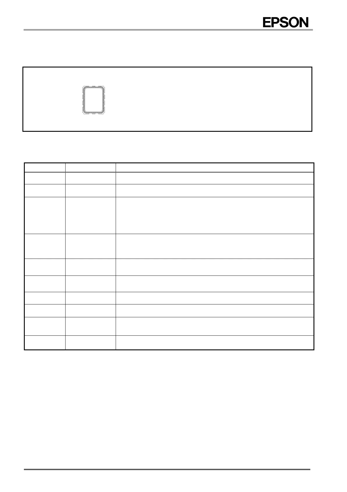
Figure 2 Package Pin layout
3.2. Pin Functions
Table 1 Pin Description
Data input and output pin.
Trigger input for Time stamp request. Built-in the programmable pull-up/down
resister.
Input detection is available in backup mode.
The reference of the input level is V
OUT
voltage. Note, there is not it with a V
IO
.
An input chattering filter rate is selectable.
When not using EVIN, connect EVIN to V
DD
or GND; don’t leave EVIN pin floating.
Frequency output pin (CMOS)
(frequency selection: 32.768 kHz, 1024 Hz, 1 Hz)
When output is stopped, the FOUT pin is High impedance.
This pin is used to output alarm signals, timer signals, time update signals, and other
signals. This pin is an N-ch open drain
Power-supply pin
Possible to supply different voltage from V
IO
Interface power supply pin
Input to supply the voltage same as a host
Internal voltage output pin
Connect bypass capacitor of 1.0 F
This is a power supply pin for backup battery
Connect an EDLC, a secondary battery, a primary battery
In the backup voltage range, supplied to IC, from this pin
Note: Be sure to connect a bypass capacitor rated at least 0.1 μF between V
DD
and GND.
For the input terminal except EVIN, it is permitted for the input to be 5.5 V regardless of the V
IO
voltage.
For the Open-Drain pin, it is permitted for the pull-up to be 5.5 V regardless of the V
IO
voltage.