1.4.2.
Power-on Sequence and Power Reset
Power-on Sequence
ESP8266EX uses 3.3 V as the system power supply. It is not allowed that Pin7 CH_EN be
powered on prior to that the 3.3 V system power supply is powered on.
Reset
Pin32 serves as a RST pin which can be dangled when it is not used. The reset pin is held low
level when the chip is enabled. In order to avoid reset caused by external interference, the lead
is generally required to be short, and no external pull-up resistor is necessary.
Pin7 CH_EN can also be used as a reset pin. When the voltage for CH_EN pin is low, the chipset
will be powered off.
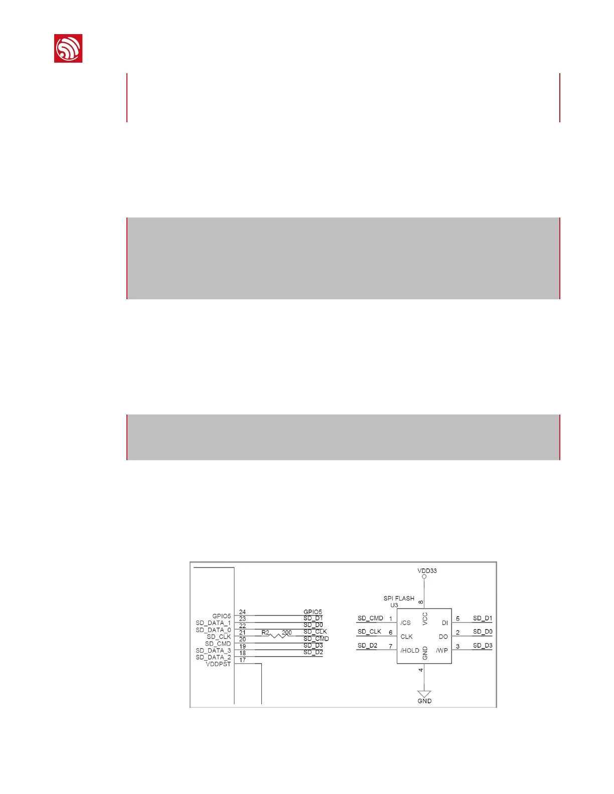
1.4.3.
Flash
The demo flash used by ESP8266EX is SPI Flash with 2 MB ROM in SOIC_8 (SOP_8) package.
Pin21 SD_CLK is connected to the Flash CLK pin together with a 0402 resistor in serial
connection to reduce the drive current and eliminate external interruption. The initial
resistance of the resistor is 200 Ω.
Figure 1-6: ESP8266EX Flash
Note:
ESP8266EX’s EMC is in conformity with FCC and CE requirements, there is no need to add ferrite
beads in analog power-supply circuit.
⚠Notice:
If the power management IC is connected with the power-on enable pin CHIP_EN, it can control the
power on-and-off of ESP8266EX by output high and low voltage through its GPIOs. However,
pulsed current might be produced at the same time. In order to delay the transmission of pulsed
signal and avoid unstable current of CHIP_EN, a RC time-delay circuit (R=1 kΩ, C=100 nF) is needed.
 Loading...