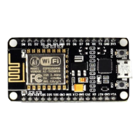
The interfaces on ESP-LAUNCHER are described in Table 2-2.
USB interface provides 5 V power supply which can be converted to 3.3 V through DC/CD
converter. One light indicating the power, and a skip stitch for testing the power current.
Three slide switches are used for 5 V power supply (Figure 2-1-8), GPIO0 voltage level switch
(Figure 2-1-9) and chip enable pin CH_EN (Figure 2-1-10). When a switch is pulled up, the voltage
level is high. When a switch is pulled down, the voltage level is low.
Pull up the power switch to power on the board, and pull down the switch to power off the board.
Pull up the GPIO0 switch to enter Flash boot mode. UART debug tool can be used to debug. Pull
down the GPIO0 switch to enter UART Download mode to download software to Flash through
ESP Flash Tool.
SW1 is connected to MTCK (GPIO13) for application reset including reset Wi-Fi configurations
(Figure 2-1-2). SW2 is not defined (Figure 2-1-22).
Red light (D2) indicates Wi-Fi work status (Figure 2-1-3).
Blue (D3) indicates communication with server (Figure 2-1-3).
Green light (D1) is an indicator light for relay switch control (Figure 2-1-15)
Blue light (D11) and red light (D10) indicate Rx and Tx work status (Figure 2-1-7)
Red light (D12) indicates 5 V power supply (Figure 2-1-8).
D4/13/14/16 are to be defined (Figure 2-1-22).
J82: It needs to be short-circuited by a jumper, so 3.3 V power supply can be connected to other
circuits. It can also be used to test power current (Figure 2-1-14).
J3: Chip select for HSPI flash. HSPI flash is disabled when the upper two pins are short-circuited
by a jumper. HSPI flash is enabled when the bottom two pins are shorted circuited by jumper
(Figure 2-1-12).
J14 and J67: Short circuit J14 to connect GPIO13 to U0CTS. Short circuit J67 to connect GPIO15 to
U0RTS (Figure 2-1-6).
J77: Short circuit J77 to connect GPIO16 to EXT_RSTB to awake the device from deep sleep (Figure
2-1-26).
UART, HSPI, SDIO/SPI, I2C, ADC_IN, GPIO16, relay control, PWM and IR TX/RX
Flash1 (the one mounted on the test board): Flash1 is connected to the chipset using SPI interface.
Currently, Flash1 is mainly used when the chip is working under WiFi standalone mode. R9 and
R85 can be used as chip select of Flash1. By default, Flash 1 is enabled (Figure 2-1-18).
Flash2 (the one mounted on the baseboard): Flash2 is connected to the chipset using HSPI
interface. HSPI is mainly used in SIP mode, in this application, ESP8266EX chipset is used as slave
device, and is connected to the host MCU using the SPI interface that is defined in standard SDIO
interface. HSPI is connected to Flash2. J3 can be used as chip select of Flash2 (Figure 2-1-11).
There are several modules that can be connected with ESP-LAUNCHER development board for
testing and development, including the test board that is mounted on the baseboard, modules
with1.27mm double-row needles (Figure 2-1-23), and 2.00mm double-row needles.
It should be noted that pins of the modules should be connected with corresponding pins on the
baseboard. Besides, only one type of module can be used at one time.
 Loading...