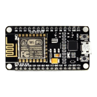
RF Antenna Interface!
Chip Output Impedance = 50 Ω!
No matching required. It is suggested to retain the π-type
matching network to match the antenna.
Amplifier power: 3.0 V ~ 3.6 V
Amplifier power:3.0 V ~ 3.6 V
ADC pin. It can be used to test the power-supply voltage of
VDD3P3 (Pin3 and Pin4) and the input power voltage of
TOUT (Pin 6). However, these two functions cannot be used
simultaneously.
Chip Enable
High: On, chip works properly
Low: Off, small current consumed
Deep-sleep wakeup (need to be connected to EXT_RSTB;
GPIO16
Digital / IO power supply (1.8 V ~ 3.3 V)
GPIO13; HSPI_MOSI; UART0_CTS
GPIO15; HSPI_CS; UART0_RTS
UART Tx during flash programming; GPIO2
Digital / IO power supply (1.8 V ~ 3.3 V)
Connect to SD_D2 (Series R: 200 Ω); SPIHD; HSPIHD;
GPIO9
Connect to SD_D3 (Series R: 200 Ω); SPIWP; HSPIWP;
GPIO10
Connect to SD_CMD (Series R: 200 Ω); SPI_CS0; GPIO11
Connect to SD_CLK (Series R: 200 Ω); SPI_CLK; GPIO6
Connect to SD_D0 (Series R: 200 Ω); SPI_MSIO; GPIO7
Connect to SD_D1 (Series R: 200 Ω); SPI_MOSI; GPIO8
UART Rx during flash programming; GPIO3
UART Tx during flash programming; GPIO1; SPI_CS1
Connect to crystal oscillator output, can be used to provide
BT clock input
Connect to crystal oscillator input
 Loading...