VS AND Vd ADJUSTMENT
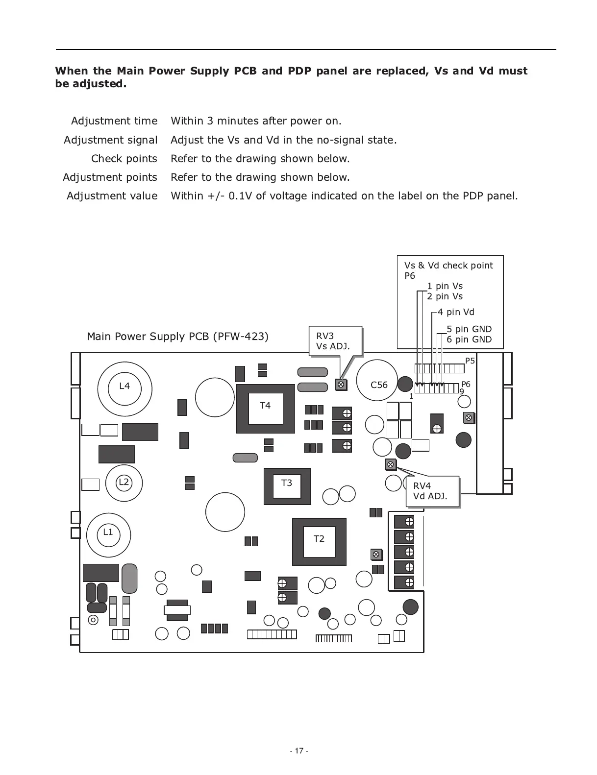
When the Main Power Supply PCB and PDP panel are replaced, Vs and Vd must
be adjusted.
Adjustment time Within 3 minutes after power on.
Adjustment signal Adjust the Vs and Vd in the no-signal state.
Check points Refer to the dra wing shown below.
Adjustment points Refer to the drawing shown below.
Adjustment value Within +/- 0.1V of voltage indicated on the label on the PDP panel.
Vs & Vd check point
P6
T4
T3
T2
L4
L2
L1
P5
P6
C56
RV3
Vs ADJ.
RV4
Vd ADJ.
1
9
1 pin Vs
2 pin Vs
4 pin Vd
5 pin GND
6 pin GND
Main Power Supply PCB (PFW-423)
 Loading...