User Guide
GD32E507Z-EVAL
21/43
5.9. ADC0_ADC1_Regular_Parallel_mode
5.9.1. DEMO purpose
This demo includes the following functions of GD32 MCU:
Learn to use the ADC to convert analog signal to digital data
Learn to use ADC0 and ADC1 regular parallel mode
5.9.2. DEMO running result
Download the program <09_ADC0_ADC1_Regular_Parallel_mode> to the GD32E507Z-
EVAL-V1.0 board. Connect serial cable to USART0, open the HyperTerminal. PC2 and PC3
pin connect to external voltage input.
TIMER1_CH1 is the trigger source of ADC0 and ADC1. When the rising edge of
TIMER1_CH1 coming, ADC0 and ADC1 convert the regular channel group parallelly. The
values of ADC0 and ADC1 are transmitted to array adc_value [0] and adc_value[1] by DMA.
When the first rising edge of TIMER1_CH1 coming, the value of the ADC0 conversion of PC2
pin is stored into the low half word of adc_value[0], the value of the ADC1 conversion of PC3
pin is stored into the high half word of adc_value[0]. When the second rising edge of
TIMER1_CH1 coming, the value of the ADC0 conversion of PC3 pin is stored into the low half
word of adc_value[1], the value of the ADC1 conversion of PC2 pin is stored into the high half
word of adc_value[1].
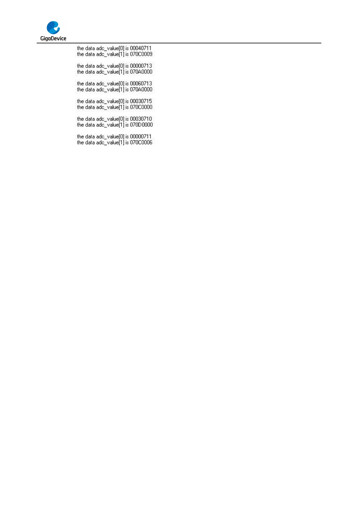
When the program is running, HyperTerminal displays the regular value of ADC0 and ADC1
stored in adc_value [0] and adc_value [1].
 Loading...