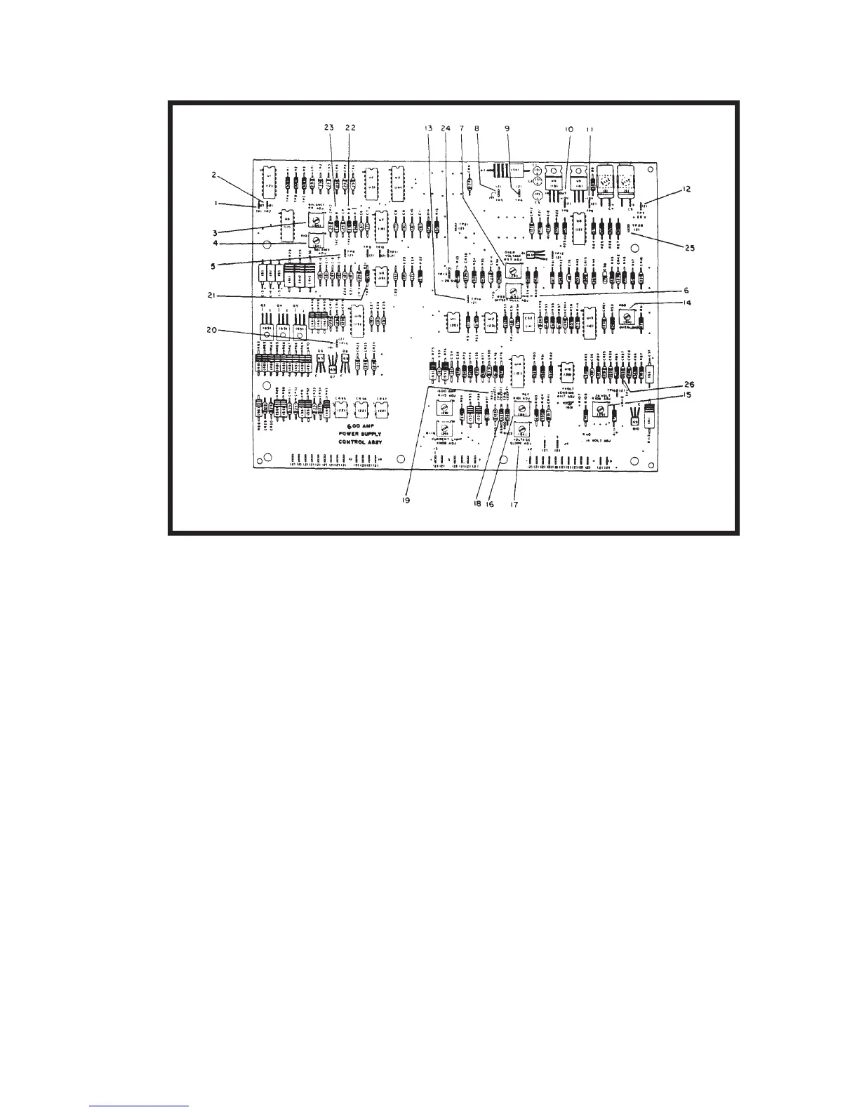
1. TP1 SCR Gate Pulse from R10 13 TP14 Null at 0 A DC TP, (R38) *
Adjust. 14. R60 Overload Limit, (TP20)
2. TP2 SCR Gate Pulse from R9 15. R109 28 V DC Output Cal., (TP13)
Adjust.
3. R9 Balance Adjust. Phase 2, 16. R101 5 V Ref Volt Adjust., (TP19)
(TP2) 17. R102 Voltage Slope Adjust.,(TP17)
4. R10 Balance Adjust. Phase 3, 18. TP19 Reference Volt Test Point,
(TP1) (R101)
5. TP8 Balanced SCR Gate Pulse, 19. TP17 Voltage Slope Test Point,
Phase 1 (R102)
6. R38 No Load Amp OFF Set Null, 20. TP15 Common, PC Board Volts
(TP14)* 21. TPF SCR Gate Pulse Timer
7. R37 Overvoltage Trip Point 22. TPE Gate Timer Output, Phase 2
8. TP3 PC Board Common 23. TPD Gate Timer Output, Phase 3
9. TP4 + 9.1 V DC Timer Voltage 24. TP13 Actual Output Volts
10. TP5 + 15 V Regulated Voltage (28.5 or 14.25)
11. TP6 - 15 V Regulated Voltage 25. TP20 Overload Limit (R60) Adjust
12. TP7 + 24 V Nonregulated
Voltage 26. TPL Overload Trip Summing Point
* Note: TP14 provides amplified load Amp reading for comparison with overload limit (TP20) and starting
amperage limit (TP21) set by R13 control on front panel.
Printed Circuit Control Board Test Points
Figure 1
OM-2010
April 10/89 Revised 3-3
Page 3