Model
333A/334A
Section IV
(5
E IN
0
~
TYPICAL WlEN
BRIDGE
I
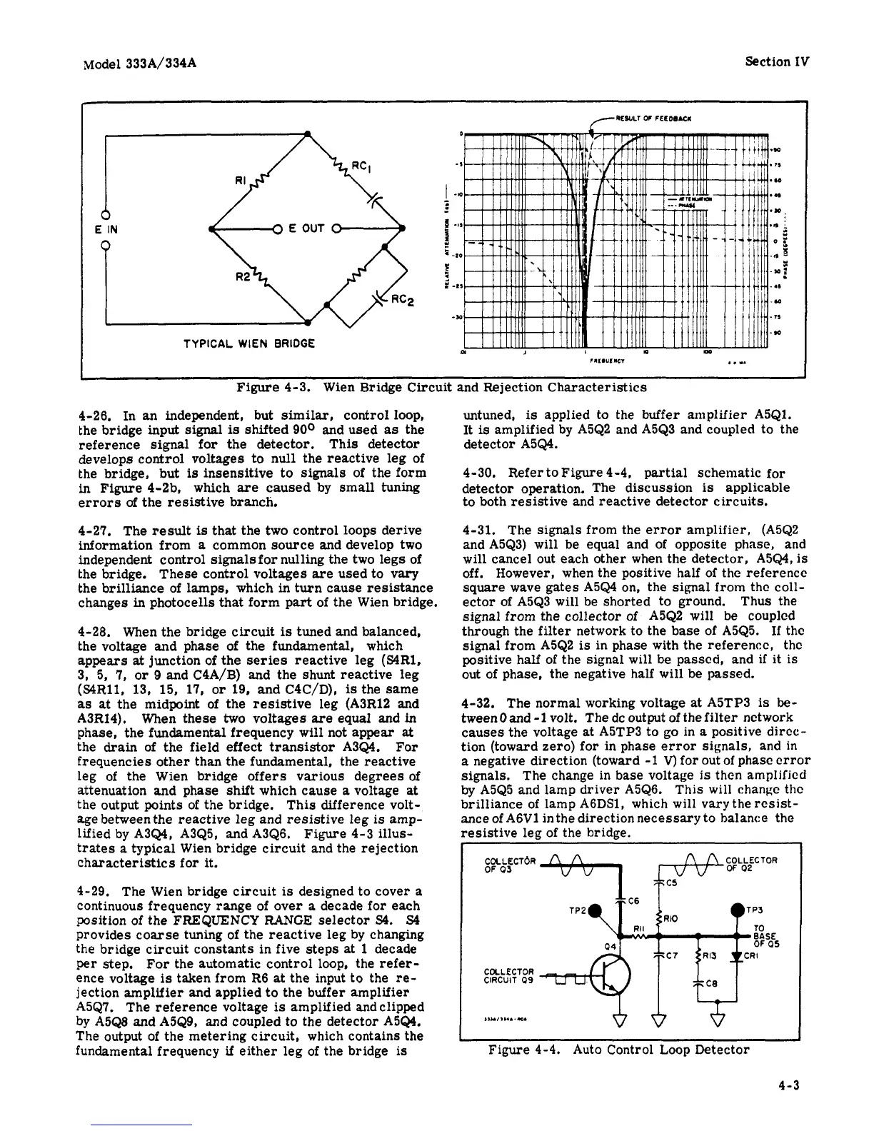
Figure
4-3.
Wien Bridge Circuit and Rejection Characteristics
4-26.
In
an
independent, but similar, control loop,
the bridge input
signal
is
shifted
900
and used
as
the
reference
signal
for the detector. This detector
develops control voltages to null the reactive leg of
the bridge, but
is
insensitive to signals of the form
in
Figure
4-2b,
which
are
caused by small tuning
errors
of
the
resistive branch.
4-27.
The
result
is
that the two control loops derive
information from
a
common source and develop two
independent control signalsfor nulling the two legs
of
the bridge. These control voltages are used to vary
the brilliance of lamps, which
in
turn cause resistance
changes
in
photocells
that
form part of
the
Wien bridge.
4-28.
When the bridge circuit
is
tuned and balanced,
the voltage and phase
of
the fundamental, which
appears
at
junction of the
series
reactive leg
(SQR1,
3, 5,
7,
or
9 and
C4A/B)
and the shunt reactive leg
(SQRll, 13, 15, 17,
or
19,
and
C4C/D),
is
the
same
as
at
the midpoint of the resistive leg
(A3R12
and
A3R14).
When
these
two
voltages
are
equal
and
in
phase, the fundamental frequency will not appear
at
the drain of the field effect transistor
A3Q4.
For
frequencies other than the fundamental, the reactive
leg of the Wien bridge offers various degrees
of
attenuation and phase shift which cause a voltage at
the output points of
the bridge. This difference volt-
age
between the reactive leg and resistive leg
is
amp-
lified by
A3Q4, A3Q5,
and
A3Q6.
Figure
4-3
illus-
trates a typical Wien bridge circuit and the rejection
characteristics for
it.
4-29.
The Wien bridge circuit
is
designed
to
cover
a
continuous frequency range of over a decade for each
position of the
FREQUENCY
RANGE
selector
S4.
S4
provides coarse tuning
of
the
reactive leg by changing
the bridge circuit constants in five steps at
1
decade
per
step.
For
the automatic control loop, the refer-
ence voltage
is
taken from
R6
at the input to the re-
jection amplifier and applied to
the
buffer amplifier
A5Q7.
The reference voltage
is
amplified and clipped
by
A5Q8
and
A5Q9,
and coupled to the detector
A5Q4.
The output of the metering circuit, which contains the
fundamental frequency
if
either leg of the bridge
is
untuned,
is
applied to the
buffer
amplifier
A5Q1.
It
is
amplified by
A5Q2
and
A5Q3
and coupled to the
detector
A5Q4.
4-30.
Refer to Figure
4-4,
partial scheiiiatic
for
detector operation. The discussion
is
applicable
to both resistive and reactive detector circuits.
4-31.
The
signals
from the error amplifier,
(A5Q2
andA5Q3)
will
be
equal and of opposite phase, and
will
cancel out each other when
the
detector,
A5Q4,
is
off. However, when the positive half of the referencc
square wave gates
A5Q4
on,
the
signal from thc coll-
ector of
A5Q3
will
be shorted to ground. Thus the
signal from the collector
of
A5Q2
will
be
couplcd
through the filter network to
the base of
A5Q5.
If
thc
signal from
A5Q2
is
in phase with the referencc, thc
positive half of the signal
will
be
passcd, and
if
it
is
out of phase, the negative half will
be
passed.
4-32.
The normal working voltage at
A5TP3
is
be-
tween0 and
-1
volt. The dc output of the filter nctwork
causes the voltage
at
A5TP3
to go in
a
positive dircc-
tion (toward zero) for in phase error signals, and
in
a
negative direction (toward
-1
V)
for
out of phase
error
signals. The change in base voltage
is
then ampIificd
by
A5Q5
and lamp driver
A5Q6.
This
will
change thc
brilliance of lamp
A6DS1,
which
will
vary
the resist-
ance of
A6V1
in the direction necessary to balance the
resistive leg of the bridge.
I
I
I I
I-1
I
Figure
4-4.
Auto
Control
Loop
Detector
4-3