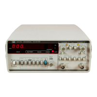
Model 5315A/B
Service
8-6
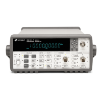
8-31. Overall Block Theory
6-
32.
T
he
53
15
A/ B U
ni
versal Coun
te
r is
co
mprised of the follow
in
g function
al
block
s:
a. Input Channels (
A&B
)
b. M
ul
tiple-Regist
er
-
Co
unter (MRC)
c.
Microcomputer
d. Display/Ex
pon
e
nt
Decoder Drivers
e. Display
f.
Function
Sw
itches
g.
P
ower
Supply
6-
33.
There are two basically identical input channel
s,
w
hi
ch condition and shape the input
signal
s.
Fr
ont panel controls allow indiv
id
ual selection of
AC
/
DC
coupling, A
TTE
N,
SLO
PE,
and
SEP
/ COM A configura
ti
on
. Input ampl
if
iers and
co
mparators buffer and
square
the
signals,
and set
the
des
ir
ed
trigger level (or sehs
it
iv
it
y). The signals are
the
n level
-s
hift
ed
and input to
the MRC as Channel A and Channel
B.
T
he
MRC receives inputs from Channels A and
Band
the r
eference
oscillator, and
then,
via
commands from t
he
j.l.C
, performs the data
co
llection for
th
e
fu
nction
mode
specified by front panel
contro
l
s.
6-34.
To
make a measur
ement,
the microcomputer routinely scans and stores the Function
Switches, and then
co
n
fig
ures the MRC, via
the
A
ddre
ss/Command bus,
to
the
desired measure-
ment
mode
(i.e., frequency, period, t
im
e i
nte
r
va
l, tota
li
ze, etc.). It then "arms"
the
MR
C,
which
allows the me
as
urem
ent
to begin.
Th
e input signal to
the
MRC starts the measur
eme
nt, and when
the
Gate
Tim
e One-Shot
ti
mes out, the MRC signals
the
microcomputer (v
ia
IR
Q) that
the
measur
eme
nt is c
omp
lete. The micr
oco
m
pute
r w
ill
then read
the
measur
ement
data from
th
e
MRC, manipulate
it
if
necessary and
then
direct
it
to t
he
Display Driver. The
Di
splay Driver
r
ece
ives, decodes. and
then
displays
the
data. The
exponent
,
exponent
s
ig
n, and decimal point
are
si
multaneously
comp
uted within the microcomputer and d
isp
layed, along with th
eappropr
i-
ate annu
nci
ato
r.
D
epe
nding
on
the function mode, the microcomputer w
ill
then typica
ll
y
reconfigure t
he
MRC and repeat the cycle un
til
the
Functi
on
Switches are changed.
6-35.
The power supp
ly
prov
id
es
three
regulated voltage
s;
+
5V
dc, +
3V
dc
, and -5.2V dc, and an
unreg
ul
ated
""
+
9V
dc
for use with options.
6-36. Assembly Circuit
Theory
6-37. T
he
following paragraphs r
eferen
ce
the schematic diagrams
in
Figures 8-7 through 8-9
and describe
the
detailed circuit theory.
8-
38.
A1
Motherboard
6
-3
9.
Th
e
motherboard
assem
bl
y contains the microcomputer, m
ul
tiple r
eg
ist
er
cou
nter,
function
sw
itches,
in
ternal oscillator and power s
upp
ly
. The m
ic
r
oco
mputer runs at an internal
clock rate of
""
2.5
MHz,
as
set by
Ll.
It continua
ll
y cycles thr
oug
h programm
ed
r
ou
tines, wh i
ch
are
st
or
ed
in
ROM with
in
the
IC T
he
block of
fundio
n
sw
itc
he
s are routi nely polled, via
the
Sw
itch Status bus, and
the
status image is stored in
in
tern
al
RAM.
Any change in the image
is
detected
, and verified. A new function
sw
itch setting must remain
st
ab
le
fo
r
32
scans to
be
accepted.