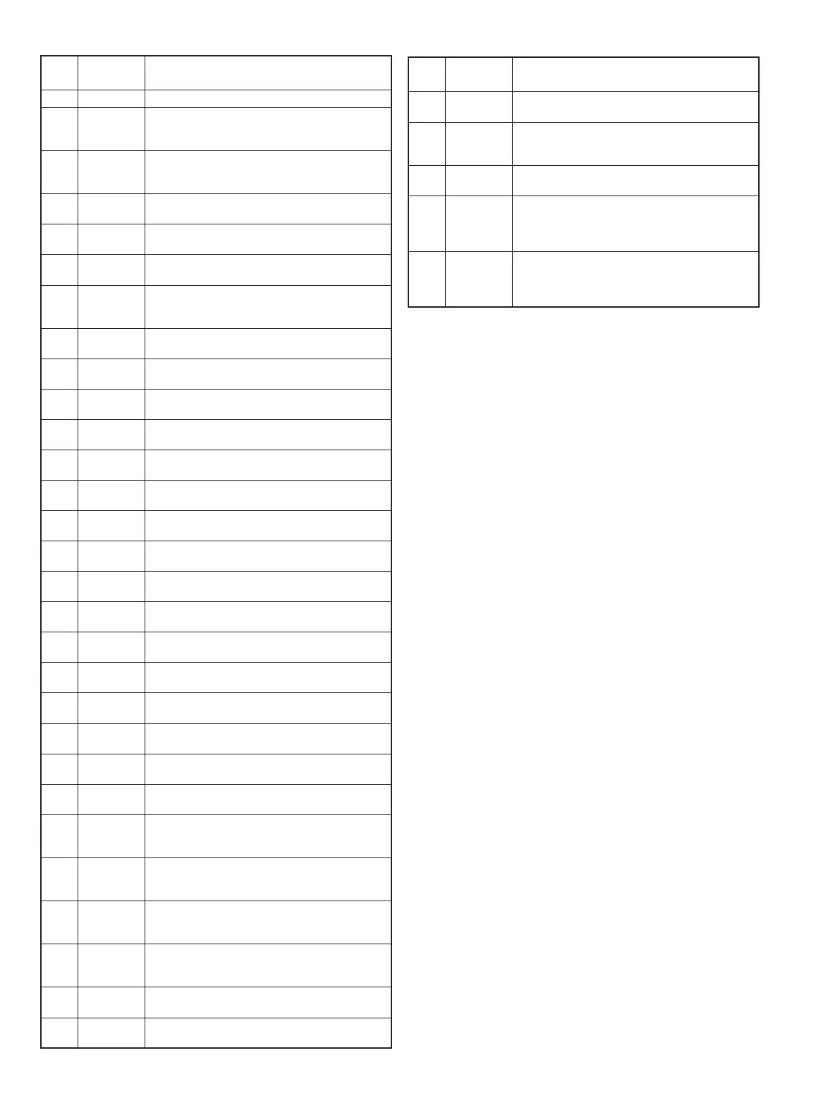
5 - 10
Pin
No.
Port
Name
Description
44 DTMF Outputs DTMF/beep/1750 Hz tone signals.
45 BTONE
Input port for tone signals (B_BAND; CTCSS,
DTCS, etc.) from the tone selector (MAIN UNIT;
IC703).
46 ATONE
Input port for tone signals (A_BAND; CTCSS,
DTCS, etc.) from the tone selector (MAIN UNIT;
IC703).
47 S-LV
Input port for RSSI signal from the D/A
converter (MAIN UNIT; IC700).
48 VOL
Input port for audio level setting signal from the
volume controller (MAIN UNIT; S702).
49 BRSSI
Input port for RSSI signal (B_BAND) from the IF
IC (MAIN UNIT; IC200).
50 TEMP
Input port for transceiver’s temperature
detection signal from the detecting temperature
selector (IC50).
51 VIN
Input port for the volatge level from the
connected power supply.
59 RESET
Input port for reset signal from the reset IC
(IC100).
69 CLSFT
Outputs CPU clock frequency shift signal to the
clock frequency oscillator (X1, D103).
70 ACQ
†
Outputs ACQ signal to the modem IC (UT-121;
IC202).
71 DCEL
†
Outputs DSEL signal to the modem IC (UT-121;
IC202).
72 RXCK
†
Input port for RX clock signal from the modem
IC (UT-121; IC202).
73 RXDT
†
Input port for RX data to the modem IC (UT-121;
IC202).
74 TXDT
†
Outputs TX data to the modem IC (UT-121;
IC202).
75 TXCK
†
Input port for TX clock signal from the modem
(UT-121; IC202).
83 TX232
Outputs data signal to the RS-232C driver
(IC52).
84 RX232
Input port for data signal from the RS-232C
driver (IC52).
85 AMBECLK
†
Outputs AME clock signal to the DSP IC
(UT-121; IC101).
86 AMBERES
†
Outputs AME reset signal to the DSP IC (UT-121;
IC101).
87 IOSTB3
Outputs strobe signal to the D/A converter
(MAIN UNIT; IC701).
88 AMBESTB
†
Outputs AME strobe signal to the DSP IC
(UT-121; IC101).
89 AMBEEPR
†
Input port for AMEEPR signal from the DSP IC
(UT-121; IC101).
90 DVC
Outputs +3D line control signal to the 3.3 V
regulator (UT-121; Q50, Q51).
“Low”=During DV
†
mode operation.
91 D_AS
Outputs mode select signal to the mode switch
(IC301).
“Low”=During DV
†
mode operation.
92 BPS
Outputs power control signal to the B_BAND
PLL IC (MAIN UNIT; IC400).
“Low”=During in power save mode.
93 UNLK
Input port for unlock signal from the PLL IC (RF
UNIT; IC800).
“Low”=While the PLL is unlocked.
94 PLLDATA
Outputs data signal to the PLL IC’s (MAIN UNIT;
IC400, RF UNIT; IC800).
95 BPLSTB
Outputs strobe signal to the PLL IC (MAIN
UNIT; IC400).
Pin
No.
Port
Name
Description
96 IOSTB2
Outputs strobe signal to the D/A converter
(MAIN UNIT; IC702).
97 AFON
Outputs AF power amplifi er control signal to the
AF6V regulator (Q105, Q106).
“High”=While the squelch is open.
98 APLLSTB
Outputs strobe signal to the A_BAND PLL IC
(RF UNIT; IC800).
99 TXC
• Outputs transmitter circuit control signal to the
LED driver (Q200) and the T5 regulator
(MAINUNIT; Q650–Q652)
“High”=While transmitting.
100 MICC
Outputs microphone amplifi er (Q302) and ALC
circuit (IC301) control signal to the microphone
amplifi er driver (Q300).
“Low”=While transmitting.
5-6 CPU PORT ALLOCATION (continued)
†
Available for the IC-91AD or when UT-121 is installed into
the
IC-91A.