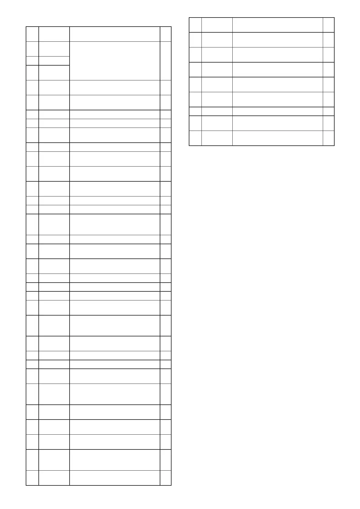
4 - 8
Pin
No.
Line
name
Description I/O
1–
11
SEG23–13
LCD segment ports. O 13 SEG12
15–
25
SEG11–1
26 SO
Serial data to DAC (M: IC6) and
audio strage IC (M: IC18).
O
27 SCK
Serial clock to DAC (M: IC6) and
audio strage IC (M: IC18).
O
28 MDIO Data I/O for baseband IC (M: IC10). I/O
29 MSCK Clock to the baseband IC (M: IC10). O
30 SS
Chip select signal to the Voice
strage IC* (M: IC18).
O
31 PLST Strobe signal to the PLL IC (M: IC4). O
32 SDA
Serial data to DAC and voice strage
IC* (M: IC18).
O
33 SCL
Serial clock to DAC (M: IC6) and
voice strage IC* (M: IC18).
O
34 INT
Interupt signal to voice strage IC* (M:
IC18).
O
35 EXSF Strobe to the expander (F: IC410). O
36 EXSM Strobe to the expander (M: IC12) O
37 EXOE
Output enable signal to the
expander ICs (F: IC410 and M:
IC12).
O
38 BEEP Beep sounds. O
39 MTDT
Data (MSK TX data) to the
baseband IC (M: IC10).
O
40 MTCK
Clock (for MSK TX data) to
baseband IC (M: IC10).
O
41 NOISE Noise level from FM IF IC (M: IC1). I
43 SDEC Tone signals (DTMF, 2/5tone). I
44 CDEC CTCSS/DTCS signals. I
45 VOXV
VOX detect.
"High"=start to transmit.
I
46 KR1
Key input for [UP], [P0] and [P3]
keys.
(Pulled up)
I
47 KR0
Key input for [DOWN], [P1] and [P2]
keys. (Pulled up)
I
48 BATV Battery volatge for monitoring. I
49 LVIN Lock voltage for monitoring. I
50 RSSI
RSSI voltage from FM IF IC (M:
IC1).
I
51 TEMP
Voltage divided by thermal register
(M: R190) and R191. (temperature
monitor)
I
52 OPTV
Optional unit detect.
"High"=An optional unit is connected.
I
55 UNLK
PLL unlock signal from IC4.
"Low"=PLL is unlocked.
I
59 RES
Reset signal from the reset IC (F:
IC408).
I
68 BPMAX
Beep sound level control signal to
BEEP SW (F: Q415).
"Low"=Maximum beep sound level.
O
69 RAC
Row address clock to the Voice
strage IC* (M: IC18).
O
Pin
No.
Line
name
Description I/O
70 PTT
[PTT] key (F: S401).
(Pulled up)
I
71 MDIR
Serial data I/O control signal to the
baseband IC (M: IC10).
O
72–
75
SENC3–
SENC6
2/5 tone, DTMF signals. O
78 MRDF
MSK data RX flag/flame detect
signal to the baseband IC (M: IC6).
O
79–
81
CENC0–
CENC2
CTCSS/DTCS signals. O
82 DAST Strobe signal to the DAC (M: IC6). O
88–
91
COM4–
COM1
LCD common terminals. –
92–
100
SEG32–24 LCD segment ports. O
*; [C], [F], [I], [L] only
4-6 CPU (F: IC401) PORT ALLOCATION
 Loading...