4-1-5 AF CIRCUITS (MAIN UNIT)
The demodulated AF signals from the demodulator circuits are
amplifi ed and fi ltered in AF amplifi er circuits.
The demodulated AF signals from the FM IF IC (IC170, pin 9)
are passed through the AF mute switch (IC260, pins 1, 2),
LPF (IC200, pins 8, 9) and variable register (VR BOARD;
R801) for level adjustment.
The level adjusted AF signals are passed through the
de-emphasis circuit (R286, C280, C285) to obtain −6 dB
of audio characteristic. The de-emphasized AF signals are
passed through the analog switch (IC430, pins 10, 11), and
applied to the AF power amplifier (IC401, pin 7) to obtain
0.6 W of AF output power. The power-amplified AF signals are
then output from pin 1, and applied to the internal speaker via
J251.
If an external speaker-microphone or headset is attached
to the [SP MIC] connector (MIC BOARD; J416), the
de-emphasized AF signals are passed through the analog
switch (IC430, pins 8, 9) and applied to the AF power amplifier
(IC280, pin 4) to obtain 0.2 W of AF output power. The power-
amplified AF signals are output from pin 10, and then applied
to the external speaker via the [SP MIC] connector (MIC
BOARD; J416).
4-1-6 SQUELCH CIRCUIT (MAIN UNIT)
The squelch mutes the AF output signals when no RF
signals are received. By detecting noise components in the
demodulated AF signals, the squelch circuit toggles the AF
power amplifier ON and OFF.
A portion of the demodulated AF signals from the FM IF IC
(IC170, pin 9) are applied to the D/A converter (RF UNIT;
IC190, pin 13) for level adjustment (squelch threshold
adjustment). The level-adjusted AF signals are output from pin
14, and passed through the noise filter (R174−R176, C177,
C179, C180). The filtered noise signals are then applied to
the noise amplifier in the FM IF IC (IC170, pins 7, 8) to be
amplified the noise components only.
The amplified noise components are converted into the
pulse-type signal at the noise detector section, and output
from pin 14 as the “NOISV” signal. The signal is applied
to the CPU (IC360, pin 32), and the CPU outputs “AFVS”
signal from pin 100 according to the “NOISV” signal level, to
the AF power regulator (Q230, Q231, Q401, Q540) which
toggles the AF power amplifier ON and OFF.
4-2 TRANSMIT CIRCUITS
4-2-1 MICROPHONE AMPLIFIER CIRCUITS (MAIN UNIT)
The AF signals from the microphone (MIC signals) are
fi ltered and level-adjusted at microphone amplifi er circuits.
The AF signals from the microphone are passed through
the AF mute switch (IC430, pins 1, 2).
While an external microphone is connected to the [SP MIC]
connector (MIC BOARD; J416), the mute switch shuts out
the AF signals from the internal microphone (MC1).
AF signals from the AF mute switch (IC430, pins 1, 2) are
passed through another AF mute switch (IC430, pins 3, 4),
and passed through the pre-emphasis circuit (R253, C254) to
obtain +3 dB of characteristic. The pre-emphasized signals are
then applied to the microphone amplifier (IC200, pins 6, 7). The
amplified MIC signals are passed through AF mute switch
(IC260, pins 8, 9), and are applied to the gain controller
(Q450, Q451) whitch adjust the AF signal level (=deviation)
according to the control signals (“MIC1/2/3”) from the CPU
(IC360, pins 106/107/108).
The level adjusted MIC (MOD) signals are applied to
the limiter amplifier (IC200, pins 13, 14) which limits the
amplitude of the MIC signals to prevent over deviation. The
amplitude-limited MIC signals are then passed through the
splatter filter (IC200, pins 1, 3) which suppresses the 3 kHz
and higher audio components.
The filtered MIC signals are applied to the modulation circuit
(RF UNIT; D20).
4-2-2 MODULATION CIRCUIT (RF UNIT)
The modulation circuit modulates the VCO oscillating signal
with the AF signals from the microphone.
The MIC signals from the microphone amplifier circuits
are applied to the D20, and modulate the VCO oscillating
signal by changing the reactance of D20. The modulated
VCO output signal is buffer-amplified by Q23 and Q24, then
applied to transmit amplifiers as a transmit signal via the
TX/RX switch (D50 is ON, D51 is OFF).
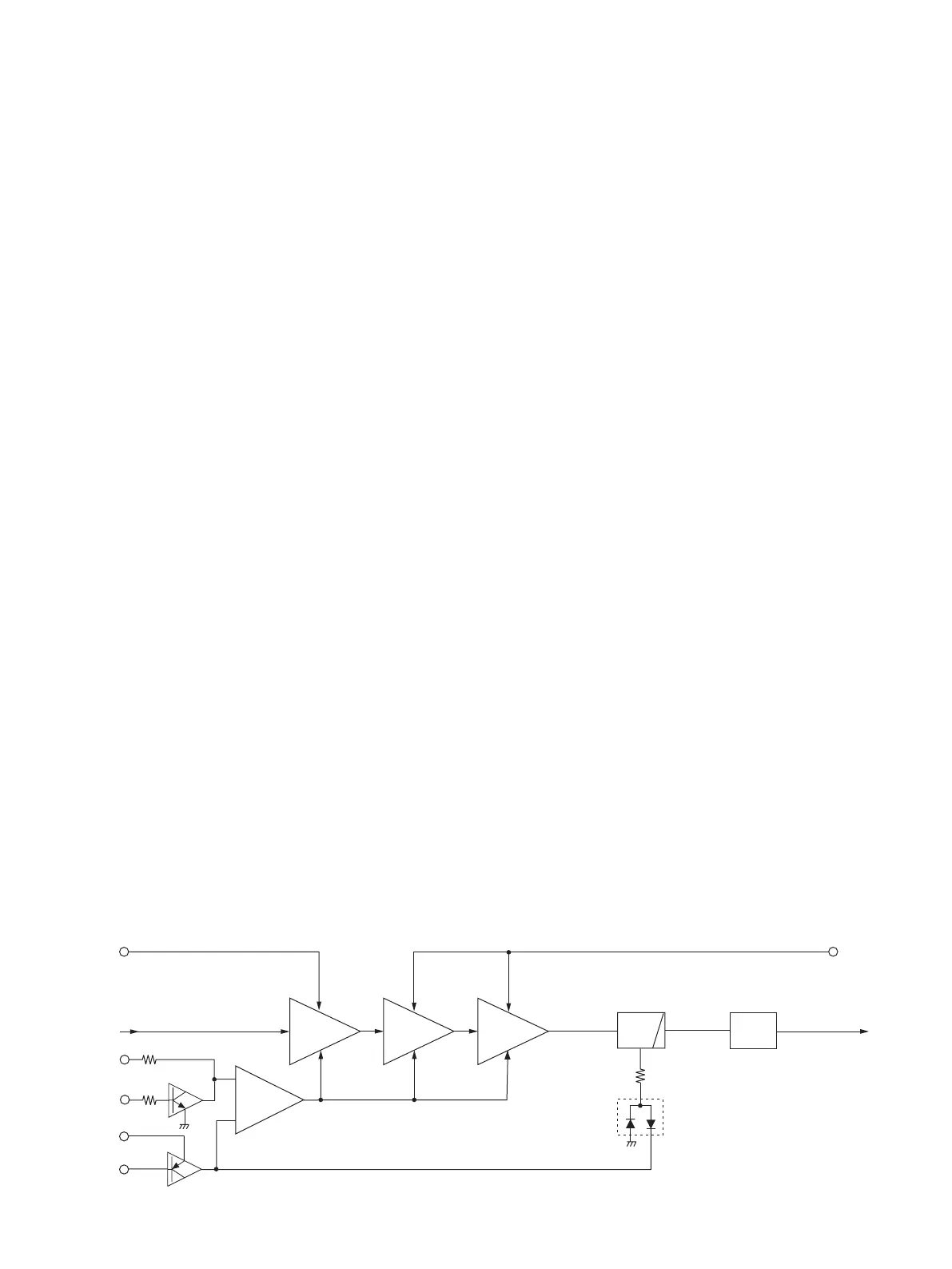
4 - 2
Power
amp.
APC
amp.
Buffer
amp.
+
–
VCC
APC CIRCUIT
to the anntena
T5V
PCON
LOW
TXMS
from the TX/RX switch (D50)
Q53
Pre-drive
amp.
Q50
IC50
3
1
4
Q17
Q54
LPF
ANT
SW
Q351
D91
D52
T5V