(c) BPF3
Receive
signals via 019 are fed
to
a HPF consisting
of
L32,
L69,
C34, C35,
C51
and C133. The cut-off
frequency
of
the HPF is
240
MHz.
The receive
signals are then input
to
the
RF
amplifier.
The input tuning
circuit
of
the
RF
amplifier
(Q3)
is
composed
of
021, 022, L33 and
L34.
The
output
tuning
circuit
is composed
of
023, 024, L36 and
L37.
These
circuits
are tuned by the tuning voltage from
IC2(A).
(d)
BPF4
Receive
signals via RL 1 are fed
to
the parallel
resonance
circuit
consisting
of
varicap 026,
L39
and
C45.
The
circuits
attenuate interference signals
to
half
of
the receive frequency.
Input and
output
tuning
circuits
of
the
RF
amplifer
are composed
of
a strip line and varicaps
027-030.
By utilizing the strip line, stable operations are main-
tained at high frequencies.
These
circuits
are tuned by the tuning voltage from
IC2(B).
4-1-4
RF
AMPLIFIER (RF UNIT)
Signals
from BPF are then applied
to
wide frequency
band
amplifier
Q7
with
a gain
of
approximately 10dB.
4·1·5
LO
TRAP (TUNED NOTCH) CIRCUIT (RF UNIT)
The
LO
trap
circuit
consisting
of
a strip line and
031-034
prevents the
1st
LO
signal leakage
to
the
ANTENNA
CONNECTOR.
The notch frequency is controlled by a control voltage
from IC3(B), matching the
1st
LO
frequency.
A LPF consisting
of
a strip line and
C78, C82,
C89
and C137 attenuates higher harmonics
of
the
1st
LO
signal.
4·1·6 1sr
LO
AND 1sr MIXER CIRCUITS (RF UNIT)
A BPF consisting
of
a strip line, L78, C134, C59,
C77
and
C53-C55
attenuates unnecessary signals from
the PLL
UNIT.
Table
2 shows the relation among receive frequencies
(FRX)
and
1st
LO
frequencies
(F1s1Lo).
RECEIVE FREQUENCY
1st
LO
FREQUENCY
FRX
[MHz]
F1stLo[MHz]
25-
89.9999
803.
7-
868.6999
1025-1089.9999
90-
249.9999
868.7-1028.6999'
1090-1249.9999
250-
519.9999
1028.7-1290.6999
1250-1519.9999
512-
999.9999
778.7-1266.6999
1512-1999.9999
Table 2
4-2
Q5 and
Q6
amplify
the
1st
LO
signal from the PLL
UNIT
to
approximately 10dBm. The
output
of
Q6
is
applied
to
IC6.
A DBM (double-balanced mixer) IC6 converts receive
signals
to
1st
IF (778.7MHz or 266.7MHz) signals.
4·1·7 1sr IF CIRCUIT
(RF UNIT)
(a)
1st
IF
AMPLIFIER
1st
IF signals from IC6 are amplified
at
QB
and they
are
applied
to
Fl1
or
Fl2.
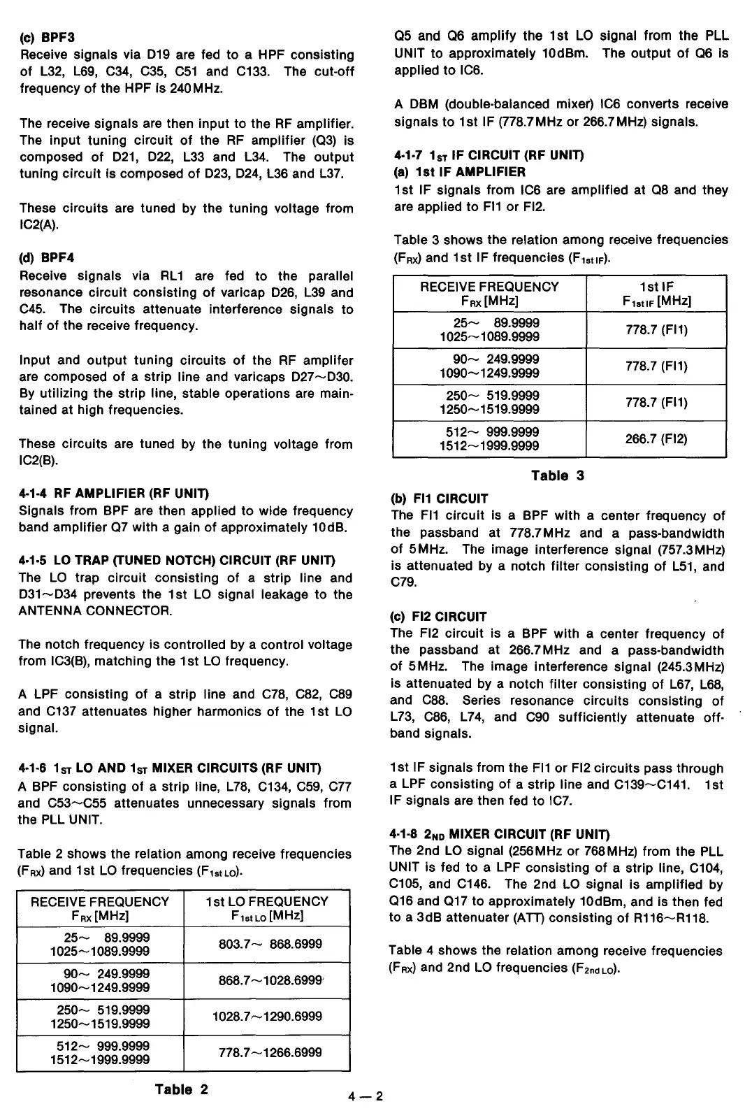
Table
3 shows the relation among receive frequencies
(FRx)
and
1st
IF frequencies
(F1st1F)·
RECEIVE FREQUENCY
1st
IF
FRX
[MHz]
F1s11F[MHz]
25-
89.9999
778.7
(Fl1)
1025-1089.9999
90-
249.9999
778.7
(Fl1)
1090-1249.9999
250-
519.9999
778.7
(Fl1)
1250-1519.9999
512-
999.9999
266.7
(Fl2)
1512-1999.9999
Table 3
(b)
Fl1
CIRCUIT
The
F11
circuit
is a BPF
with
a center frequency
of
the passband at 778.7MHz and a pass-bandwidth
of
5MHz. The image interference signal (757.3MHz)
is attenuated by a notch
filter
consisting
of
L51,
and
C79.
(c) Fl2 CIRCUIT
The
F12
circuit
is a BPF
with
a center frequency
of
the passband at 266.7MHz and a pass-bandwidth
of
5MHz. The image interference signal (245.3MHz)
is attenuated by a notch
filter
consisting
of
L67, L68,
and
C88.
Series resonance
circuits
consisting
of
L73,
C86,
L74,
and
C90
sufficiently
attenuate
off·
band signals.
1st
IF signals from the
Fl1
or
Fl2
circuits
pass through
a LPF consisting
of
a strip line and
C139-C141.
1st
IF signals are then fed
to
IC7.
4·1·8
2No
MIXER CIRCUIT (RF UNIT)
The 2nd
LO
signal (256MHz
or
768MHz) from the PLL
UNIT is fed
to
a LPF consisting
of
a strip line, C104,
C105,
and C146. The 2nd
LO
signal is amplified by
Q16 and Q17
to
approximately 10dBm, and is then fed
to a
3dB
attenuater
(ATT)
consisting
of
R116-R118.
Table
4 shows the relation among receive frequencies
(FRx)
and 2nd
LO
frequencies
(F2nd
Lo).
 Loading...