RECEIVE FREQUENCY 2nd
LO
FREQUENCY
FRx
[MHz]
F2nd
LO
[MHz]
25-
89.9999
768
1025-1089.9999
90-
249.9999
768
1090-1249.9999
250-
519.9999
768
1250-1519.9999
512-
999.9999
256
1512-1999.9999
Table 4
A double-balanced
mixer
IC7 converts
1st
IF signals
to
2nd IF (10.7MHz) signals.
A LPF
consisting
of
C142-C144
attenuates higher
harmonics
of
2nd LO signal from IC7.
Q18
amplifies
2nd IF signals from IC7, and the
output
of
Q18 is fed
to
the IF UNIT.
A part
of
2nd IF signals from IC7 is buffer-amplified
at Q19, then is
applied
to
a LPF
consisting
of
L60
and
C114-C116.
These signals are then fed
to
the
[10.7MHz
IF OUTPUT] JACK.
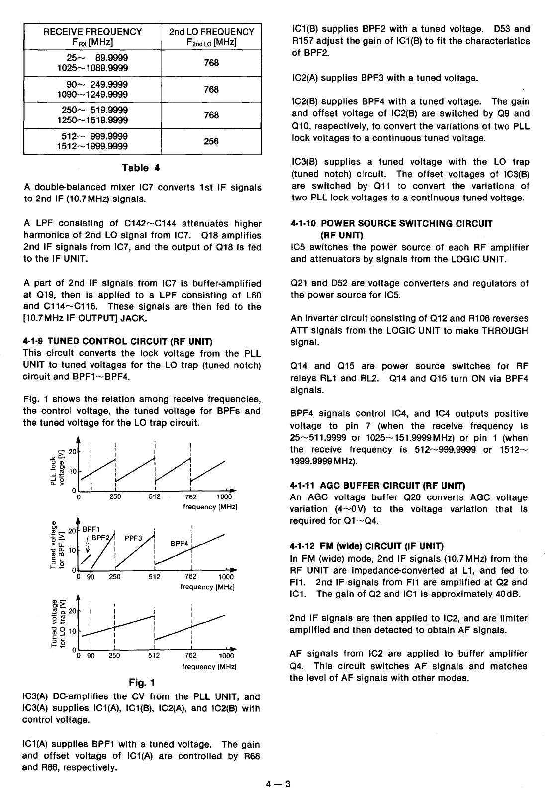
4·1·9 TUNED CONTROL CIRCUIT
(RF
UN!n
This
circuit
converts the
lock
voltage from the PLL
UNIT
to
tuned voltages
for
the LO trap (tuned notch)
circuit
and
BPF1-BPF4.
Fig. 1 shows the relation among receive frequencies,
the
control voltage, the tuned voltage for BPFs and
the tuned
voltage
for
the LO trap circuit.
I I j I
~~
::
y:
'.VJ:V1
1
V'
~-
I I I
..Jo
I
CL
> I I
0 I I
0 250 512 762 1000
frequency [MHz]
frequency [MHz]
frequency [MHz]
Fig.1
IC3(A) DC-amplifies the
CV
from the PLL UNIT, and
IC3(A) supplies IC1(A), IC1(B), IC2(A), and IC2(B)
with
control voltage.
IC1(A) supplies
E!PF1
with
a tuned voltage. The gain
and
offset
voltage
of
IC1(A) are
controlled
by
R68
and
R66,
respectively.
IC1(B) supplies
BPF2
with
a tuned voltage. 053 and
R157
adjust
the gain
of
IC1(B)
to
fit
the
characteristics
of
BPF2.
IC2(A) supplies BPF3
with
a tuned voltage.
IC2(B) supplies
BPF4
with
a tuned voltage. The gain
and
offset
voltage
of
IC2(B) are
switched
by
Q9
and
Q10,
respectively,
to
convert the variations
of
two
PLL
lock
voltages
to
a
continuous
tuned voltage.
IC3(B) supplies
a tuned voltage
with
the
LO
trap
(tuned notch) circuit. The
offset
voltages
of
IC3(B)
are switched by
Q11
to
convert the variations
of
two
PLL
lock
voltages
to
a
continuous
tuned voltage.
4·1·10 POWER SOURCE SWITCHING CIRCUIT
(RF
UNln
IC5
switches
the power source
of
each
RF
amplifier
and attenuators by
signals
from the LOGIC UNIT.
Q21
and 052 are voltage converters and regulators
of
the power source for IC5.
An
inverter
circuit
consisting
of
Q12
and
R106
reverses
ATT
signals from the LOGIC UNIT
to
make THROUGH
signal.
Q14
and
Q15
are power source
switches
for
RF
relays
RL1
and
RL2.
Q14 and
Q15
turn
ON
via BPF4
signals.
BPF4 signals control IC4, and IC4
outputs
positive
voltage
to
pin 7 (when the receive frequency is
25-511.9999
or
1025-151.9999MHz)
or
pin 1 (when
the receive frequency is
512-999.9999
or
1512-
1999.9999 MHz).
4·1·11
AGC BUFFER CIRCUIT (RF
UNln
An
AGC voltage
buffer
Q20 converts AGC voltage
variation
(4-0V)
to
the voltage variation
that
is
required
for
Q1-Q4.
4-1-12
FM (wide) CIRCUIT (IF
UNln
In
FM
(wide) mode, 2nd IF
signals
(10.7MHz) from the
RF
UNIT are impedance-converted at
L1,
and fed
to
Fl1. 2nd IF signals from
Fl1
are
amplified
at
Q2
and
IC1. The gain
of
Q2
and
IC1
is approximately 40dB.
2nd IF signals are then applied
to
IC2, and are
limiter
amplified and then detected
to
obtain
AF signals.
AF signals from IC2 are applied
to
buffer
amplifier
Q4.
This
circuit
switches
AF signals and matches
the
level
of
AF signals
with
other
modes.
4-3
 Loading...