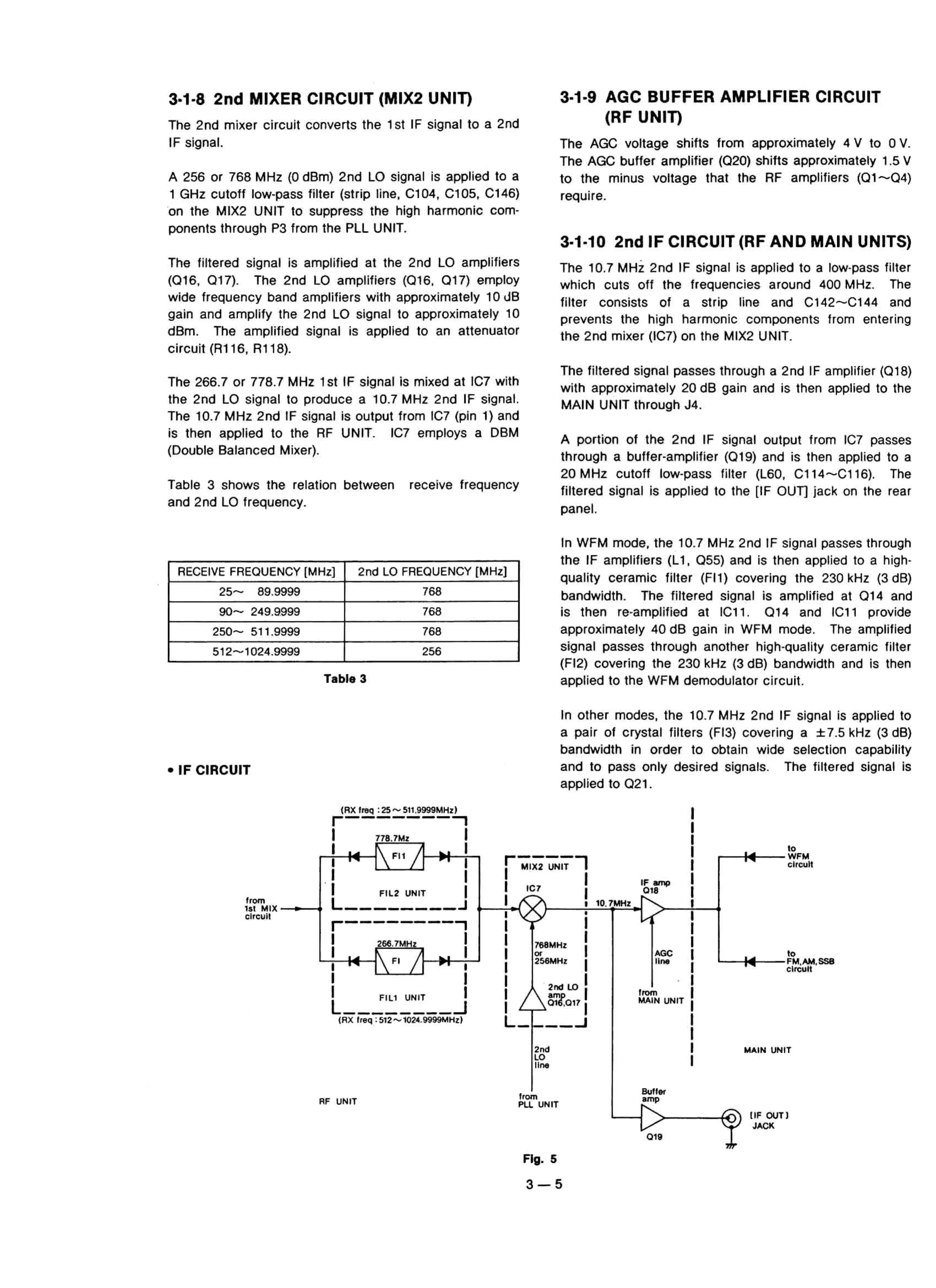
3·1·8 2nd MIXER CIRCUIT (MIX2 UNIT)
The 2nd mixer circuit converts Ihe 1
st
IF
signal
to a
2nd
IF signa
I.
A 256 or 768 MHz (0 dBm) 2nd LO signaI is applied 10 a
1 GHz cutott
lew
-pass filter (strip line,
Cl04,
C105, C146)
on the MIX2 UNIT
10 suppress
Ihe
high harmonie com-
ponents through P3 from the PLL UNIT.
The filtered signal is ampllfied
al
Ihe 2nd LO amplifiers
(016
, Q17). The 2nd LO amplifiers (Q16,
017)
employ
wide frequency band amplifiers with approximately 10 JB
gain and amplify Ihe 2nd LO signal to approximately 10
dBm
. The amplified signal is applled 10 an attenuator
circuit (R116, R118).
3·1·9 AGC BUFFER AMPLIFIER CIRCUIT
(RF UNIT)
The AGC voltage shifts from approximately 4 V 10 0 V.
The AGC buffer amplifier (020) shifts approximalely 1.5 V
to
the minus voltage thaI
Ihe
RF amplifiers
(01-04)
require
.
3·1·10 2nd
IF
CIRCUIT (RF AND MAIN UNITS)
The 10.7 MHz 2nd IF signal is applled 10 a low-pass filter
which
cuts off Ihe frequencies around 400 MHz.
The
filter consists of a strip line and C142
-C144
and
prevents Ihe
high
harmonie components
from
entering
tne 2nd mixer (IC7) on Ihe MIX2 UNIT_
The 266.7 or 778.7 MHz 1sI IF signal is mixed
al
IC7 wlth
the 2nd LO signaI to produce a
10_7
MHz 2nd IF signal.
The 10.7
MHz
2nd
fF signaI is output trom IC? (pin 1) and
is Ihen applled
10 Ihe RF UNIT_
IC7
employs a
OBM
(Double Balanced Mixer).
Tabla 3 shows Ihe relation between reeerve frequency
and 2nd LO Irequency.
The filtered signaI passes Ihrough a 2nd IF amplifier (018)
wilh
approximalely 20 dB gain and is Ihen applled to the
MAIN UNIT Ihrough J4.
A portion
of
Ihe
2nd IF signal output from IC7 passes
through a buffer-amplifier (019) and is then applied to a
20 MHz cutoft low-pass filler (L60,
Cl14
-C116
).
The
fillered
signal is applied 10 Ihe [IF
OUn
jack on the rear
panel.
RECEIVE
FREOUENCY [MHz]
2nd
LO FREOUENCY [MHz]
25-
89.9999
768
90- 249.9999 768
250- 511.9999 768
512
-10
24.9999 256
Tabla 3
In WFM mode,
lhe
10.7 MHz 2nd IF signal passes Ihrough
Ihe
IF amplltiers (1.1,
055)
and is then applied to a high·
quality
eerarme
filler
(Fll)
coverlng the 230 kHz (3 dB)
bandwidth. The filtered signal is amplified
al
014
and
is then re-amplifled at
iCl1
.
014
and
IC11
provide
appro
xlmately 40 dB gain in WFM mode. The ampllfied
signal passes through another hiqh-quallty ceramlc filter
(F12)
covering the 230 kHz (3 dB) bandwidth and is Ihen
applied
10 Ihe WFM demodulalor circuit.
•
IF
CIRCUIT
In other modes, the 10.7 MHz 2nd IF signaI is applied 10
a pair
of
crystal
filters (FI3) covering a
±7
.5 kHz (3 dB)
bandwidth
in
order to
obtain
wide selectIon capability
and to pass only desired signaIs. The
fil1ered
signal
is
applied 10 021.
FILZ
UNIT
MAIN UNIT
I.
r----I<f--
WFM
circuit
I.
'----I<f--FM
.AM
.SS8
circuit
I
I
I
I
I
I
I
I
I
I
I
AGC I
IIM
I
I
l~
I
MAIN UNIT I
I
I
I
I
'""
LO
IIM
r-;;';;;-;;;;;-l
I IC7 I
I •
10
.7~z
I X •
I I
I 768MHZ I
I
~
I
I 2!>6MHz I
I
,.dLO
I
I /
\
~
017
1
L_I-
__
...J
Fit
/
7787Mz
(RX
IntQ : 2S
......
S11
.9999MHz)
r-------...,
I
I
I I
I I
r--------...,
I "
.lM"'
I
I \ F' / I
I I
L
__
~~~:
__
J
(RX IreQ :S1
2-
1024.9999MHz)
RF
UNIT
,,~
pu. UNIT
Buller
r:
L......1
V
>-
-
---+
0'9
IIF
OUT)
JACK
Fig. 5
3-5