3·1·11 NOISE BLANKER CIRCUIT
(MAJN
UNIT)
The noise blanker circ
ui
t effec
tive
ly reduces
in
terference
trom pulse-type norse sucn as car
ign
it
ion
systems and
functions in only SSB and AM modes.
A
port
ion of the
2n
d IF signal output (drain
of
021)
Is
appli
ed
10
the noise
amp
lifier (IC14) and is then detected
at
the noise
detector
circuit
(046,
047
). The detected
voltage is applied
to
a noise blanker switch (027).
The threshold level of lhe noise blanker swi
tc
h
(027)
is
set at approximately 0.3 V higher than thaI of 0
26
to
avoid malfunctions when the operating frequency or mode
is
changed. When the detecled voltage exceeds the
tnresnold level, Q
28
output
s a blanki
ng
siçnal to activate
the
no
ise blanker
gate
circuit (0 30- 0 32).
A portion of the detected voltage
is
a
pp
lie
d la a nolse
bianker AGC circuit
(026)
. The
Ihr
eshold level of the
no
ise blanker AGC circuit (026) is set at 0.6 V. The
nolse
components are led back
la
the norse amplifier
(IC14) throu
gh
a
OC
amplifier (0 25). The time constant
of the naise blanker
AGC
circuit is determ
in
ed by R206.
R209 and C129. This AGC circuit does not det
ect
putse-
type norse.
The filter
ed
signal is
ap
plied to the 3rd IF amplifier circuit
(022
.
023)
and is then applied
10
the demodulator circuits,
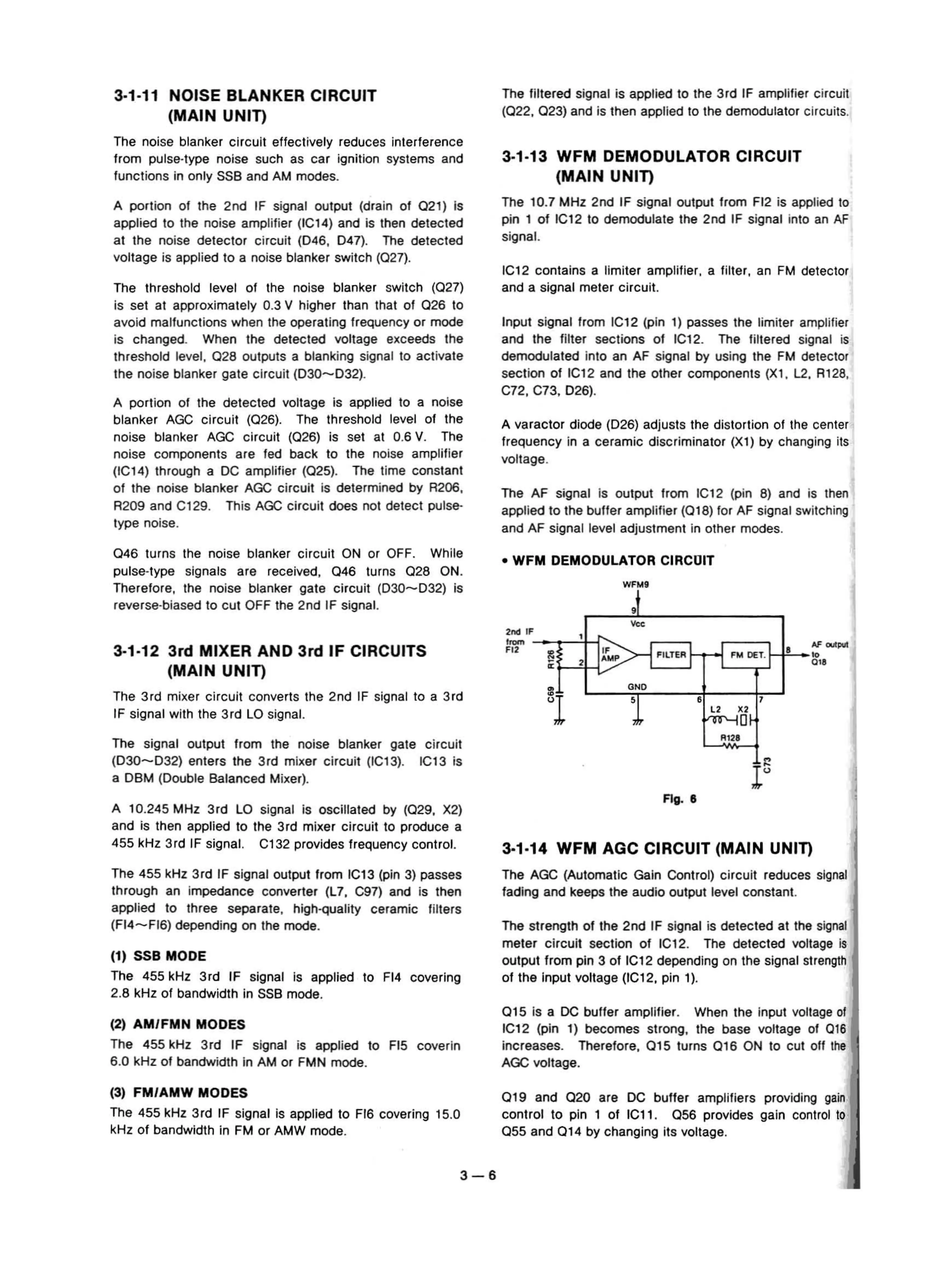
3·1·13 WFM DEMODULATOR CIRCUIT
(MAIN UNIT)
The 10.7 MHz 2nd IF signal output from FI2 is applied to
pin 1 of IC12
to
demodula
te
tne
2nd IF signaI into an AF
signa!.
IC12 contains a
li
miter amplifier, a filter, an FM detector
and
a signal meter circ
ui
t.
Input
signaI from IC12 (pin 1) passes the limiter amplif
ier
an
d the filter sections
of
IC12.
Tha
filtered signal is
demodulated into an AF signa! by using the FM detect
or
sect
ion
of
IC1
2 and the other components
(Xl,
L2
. R128,
C72. C73. 0 26).
A varactor diode (
026)
adjusts the distortion of the center
frequency in a
ce
ramic discriminator (X
l)
by changing its
voltage.
The AF signal is output from
IC1
2 (pin 6) and is then
applied
to
the buff
er
amplifier (01 6) for AF signaI switching
and
AF
signal level adjustment in other modes.
WF
M9
•
WFM
DEMODULATOR CIRCUIT
046
turns Ihe noise blanker
circuit
ON or OFF. While
pulse-type signals a
re
received, Q46 tu
rn
s Q28 ON.
Therefore.
tne naise blanker gate circuit (0
30-
D32) is
r
ever
se·bias
ed
to cut
OFF
the 2nd IF signa!.
3-1
-12 3rd MIXER AND 3rd
IF
CIRCUITS
(MAIN UNIT)
The
3rd
mixer circuit couverts the 2nd IF signal
to
a 3rd
IF signal
wit
h the 3rd LO signal.
The
signal output from the noise blanker gate circuit
(
03
0- 0 32) enters the
3rd
mixer
circu
it (IC13). IC13 is
a OBM (Double Balanced Mixer).
2
ncl
1
1"
""'"
'"
9
Vc<
,
~
"
FILTER
FM
DE
T.
•
-
,
AMP
«
•
ONO
~
l
,
, ,
L2
X
j
~
...
...,0
R128
~
A 10.245 MHz
3rd
LO signaI is oscillated by
(029
, X2)
and is then applied to the 3rd mixer circuit to produce a
455 kHz 3rd IF signal. C132 provides frequen
cy
control.
The
455
kHz
3r
d IF signaI output
fro
m IC13 (pin 3) passes
through an impedance converter C
L7.
C97)
and is then
applied to three separate, high-quality
ce
ramic
fi
lters
(FI4-
FI6) depending on the mode.
(1) SSB
MODE
The 455 kHz 3rd IF signal is applied to FI4 covering
2.6 kHz of bandwidth in SSB mode.
(2)
AM/FMN
MODES
The 455 kHz
3r
d IF signal is
app
lied
to
FIS
co
verin
6.0 kHz
of
bandw
idth in AM or FMN mode.
(3)
FM/AMW
MODES
The 455 kHz
3r
d IF signal is applied to FI6 covering 15.0
kHz
of
bandwidth in FM
or
AMW mode.
3
-6
Ag
. 6
3·1·14 WFM AGC CIRCUIT (MAIN UNIT)
The AGC (Automat
ic
Gain Control)
circui
t reduces signal
fad
in
g and keeps the audio output level constant.
The strength of the 2nd IF signal is de
tecte
d at the s
ignal
meter circuit section
of
IC12. The detected voltage
is
ou
tput
from
pin 3
of
I
C1
2 depending on the signaI strenglh
of the input voltage (IC12. pin 1).
0 15 is a
oe
buffer amplifier. When the input voltage ol
IC12 (pin 1) becomes stronç, the base
vo
ltage of Qf6
increases. Therefore, 0
15
turns
Q16
ON
to cut olf the
AGC
vo
ltage.
01
9 and 0
20
are OC buff
er
amp
lifiers providing
gai
n
con
tr
ol
to
pin 1 of IC11.
05
6 provides gain conlrol
to
0 55 and
01
4 by changing its voltage.