3·1·15 BFO AND
SSB
DEMODULATOR
CIRCUITS (MAIN UNIT)
3·1·17 AM DEMODULATOR CIRCUIT
(MAIN UNIT)
The BFO (Beat Frequency O
sc
illator) circuit consists of
Q
41
a
nd
Q42. The
os
ci
llato
r p
ro
vides a beat fre
qu
en
cy
signaI to the SSB demodulator circuit (
039-
0 42) lor
de
modulating the 3rd IF signal into an AF signal. The
BFO freque
ncy
is adjusted at L4 in SSB mode.
In LSB mode, the CPU (IC5, pin 74) on the LOGIC UNIT
outputs a " HIG
H"
signa
I.
The " HIGH" signal furns 0 40
ON. Therefore, the capacitance of
CI80
and C181 is
added to L14, C182 and C183 to increase the BFO
oscillatlon by 3 kHz.
The 3rd IF signal o
utp
ut from
023
is buffer-amplified
at 0 30 and is
th
en applied to an AM
de
modulator circu
it
(C168, 057) to be
cemod
u
ta
ted into an AF signal.
The AF signal is applied to a buffer amplifier (039)
to
r AF
sig
nal sw
it
ching and AF s
ig
nal level adjustment
in
ather
modes.
3·1·18 AM/SSB/FMN AGC CIRCUIT
(MAIN UNIT)
The AF signaI output from Ihe SSB demoduiator circuit
(
039-
04
1)
Is applied to a buffer amplifier (
02
4) for AF
signa1 switching and AF signal level adjustment in ether
modes.
3·1·16 FM DEMODULATOR CIRCUIT
(MAIN UNIT)
A portion
of
the 3rd IF signal output from 0 30 is applied
to an
AGC
detec
to
r ci
rc
u
it.
Th
e AGC voltage
is
detected
at
056
and is then applied to a OC amplifier (
03
8).
In AM or SSB mode, the
"A
M9" or "SSB9" line becomes
" HIGH
."
The
"HI
GH" signaI turns 0 34 and
035
ON.
Th
erefore, R246 shortene
th
e time co
nst
ant. C
161
end
R247
are connected in
pa
rallel
with
the
AG
C t
im
e
constant line
10
obtain an appropriate
ti
me
constant.
The 3rd IF signal output trom
023
Is buffer-a
mp
lified
at
030
and is then
appl
ied 10 a limiter amplifier (ICIS) to
elimlnate the
AM
signal components.
The
signaI output f
ro
m IC15
is
a
pp
ll
ed
to a
ce
ramie
dis
cr
iminator (X3) to be demodulated into an AF signal.
The AF signal is applied to an
ac
tive filter circuit
(03
1,
0 32) to suppress the signaIs below 300 Hz.
In FM
mo
de, Ihe
"F
M9"
line becomes "LOW."
Th
e
"L
OW" signaI turns
035
OFF. Therefore, C162 and
R246
are connec
ted
in
par
all
el
wi
th
the AGC
ti
me
co
n-
stant line 10 obtaln a reold
AGC
release time.
R248 and R249 offset the AGC voltage to approximateiy
4
V when receiving no signa
!.
When the scan is in eperation. the CPU (IC5, pin 91)
on
the LOGIC UNIT outputs a
"H
iGH" signal tor 35 msec. on
the
"IFB
K" signal line. The " HIG
H"
signal turns 0 36
and
037
ON to reset the AGC circuit.
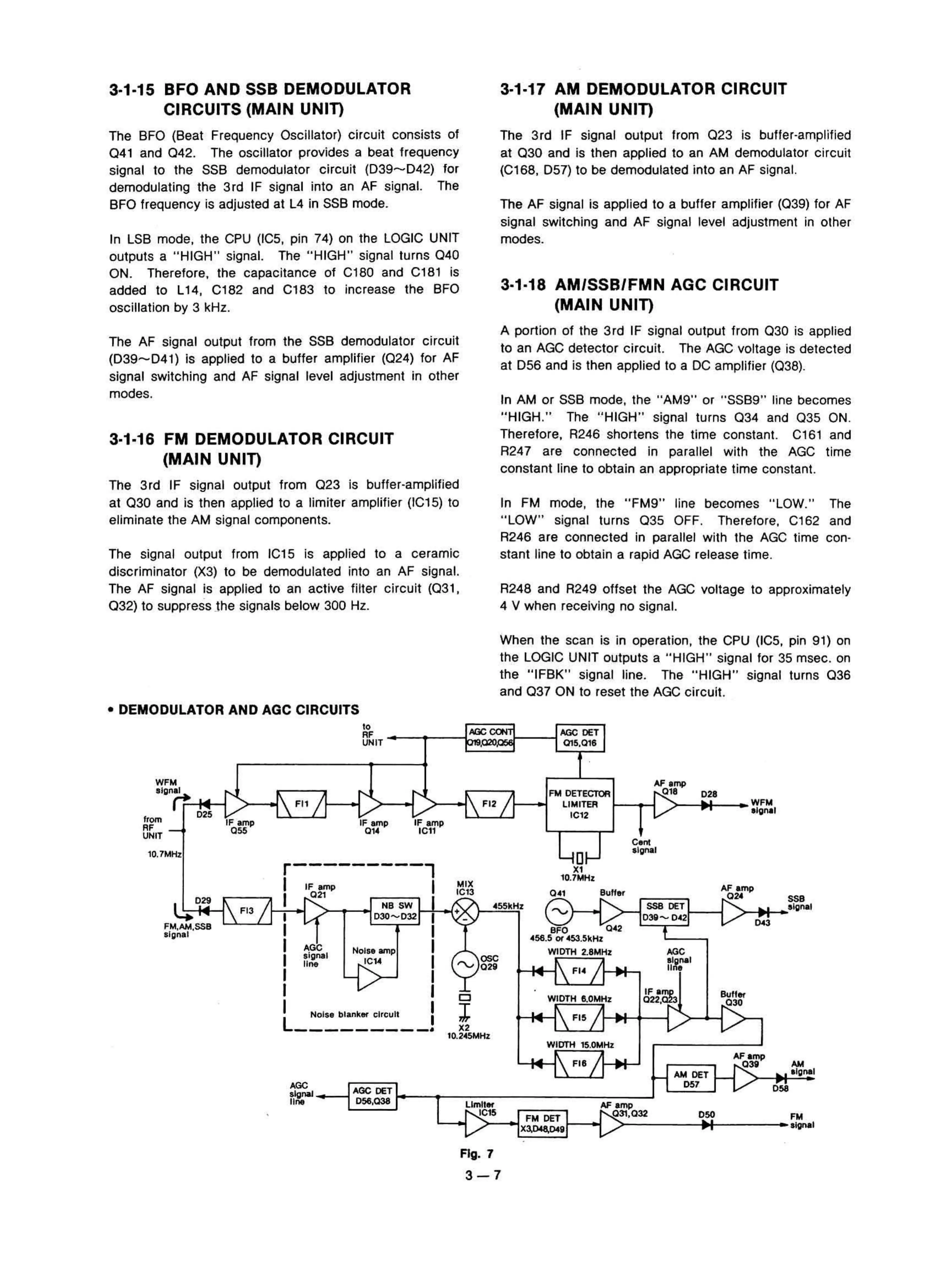
o DEMODULATOR AND AGC CIRCUITS
>IX
DET
015,01610
~-l---ê~;}---[:;~~
RF
U
NI
T
r-----r------1
AF.
mp
028
c.nt
.Ignal
o
Xl
10.
7MH:
0.1
BuHer
MIX
IC13
Fi'
r---------l
I
lF
omp I
o
AF."",
~
::-
-K~J
f-
1
FM
DETE
CTOR
0 18
?
:-
--j
~~
LJ
-
1
LIM
ITER
f-~-1
;
>-
-l
+-
_ . WFM
I
C1
2 l Ignai
IF amp
IF
Imp
A
,.
r
eu
IF
.m
p
055
029
I
~
i
"
r-,
~
.
sso
IV "/
NB SW
455k
H:
SS8
DE
T Ilgl'Ill
I
030
.....
0 32
I
'X
"V
03a
.....
0.
2
-
~2
/'
0"
.SSO
I
I
OF
O
I
I
. 56.5 Of
453
.5kH:
A
OC
Noll e amp
WI
DTH
2.8MH:
ACe
I
signai
~
,.
I
csc
sl
N.
""
IIM
"V
0 29
11
0
I
'-
V
I
è
1\
FI.
I
I
•
IFI~
&.l
il
.,
I
W
IOT
H e
.O
MH:
02
2,
~O
I
1
NolS8 b
lanker
circuIt I
FIS /
L
_________
.
.2
V
V
10
.
2.
~
Hz
W
IOTH
15.0
MHz
FIO
/
AF.mp
030
N<
l-
N<
DE
T
r-"
IlgMI
ACe
AOC
DET
OOT
V 0
..
.~.,.,
IIM
0
5&
,038
limit"
M-
Imp
• N
C15
FM DEr
1'!1.31,O32
050
FM
/'
X3,,
048.04a
V
.I
gro
ll
10
.7MHz
WFM
'l
g
~
'-+l
H
from
025
RF
UNIT
~
FM,AM
Iignal
FIg. 7
3-7