SECTION 4 CIRCUIT DESCRIPTION
4-1
RECEIVER CIRCUITS
4-1-1
RF
CONVERTOR CIRCUIT (CONV UNIT)
The RF
convertor
circuit converts 1025-1999.99999
MHz
RF
signals to
200-989.99999
MHz RF signals.
(1)
30.00000-1024.99999
MHz signals
RF signals from
the antenna connector
(J1)
pass through
the switching
relays
(RL1, RL2) to
bypass
the RF convertor
circuit. The bypassed
RF signals either
bypass or are
passed
through the RF attenuator circuit (R17-R19.
R25-R27)
then applied to the RF-B
unit via
J3.
(2)
1025.00000-1999.99999 MHz signals
RF
signals from
the
antenna connector (J1) are applied to
the
RF amplifier circuit (ICI, IC3) via the switching relay
(RL1) and
tunable high-pass filter (D3-D5, D20, D21.
L2-L4). The
amplified signals are mixed with convertor
LO
signals at the
RF convertor circuit
(1C2) to
produce
200.00000-989.99999
MHz
RF signals.
The
converted
RF
signals are applied to the RF-B unit via
J3
after bypassing
or passing through the
attenuator
circuit.
The
convertor PLL circuit (IC6; VCO, IC7: PLL
1C)
gener-
ates a 1000 or 1010
MHz
LO
signal
and
applies them
to
the
convertor circuit directly or divides them by 2 at 108.
4-1-3
VHF/UHF RF CIRCUIT
(RF-B UNIT)
The
RF circuit amplifies the received signals within the
range
of
frequency coverage
and
fitters
out-of-band signals.
The RF
circuit consists of
4
bandpass After circuits with an
RF amplifier for each.
The received signals from
the CONV
unit
are
passed
through to the tunable
bandpass filter via
the
switching relay
(RL1), then ampliAed
at
the RF ampllAer
circuit. The
amplified
RF
signals are
again passed through another
bandpass
Alter to suppress out-of-band signals. The Altered
signals are
ampliAed at the
other
RF
amplifier
circuit (IC3),
then applied to the 1st mixer circuit after passing through
the low-pass or bandpass
with tuned notch circuit.
The tunable bandpass Alters employ varactor diodes to tune
the center frequency of the RF passband for wide
band-
width receiving and
good image response rejection.
These
diodes are controlled
by
the
CPU (MAIN unit. IC33) via
the
voltage
amplifier circuit
(IC2).
A
Ga-As
FET is
used
for
the RF ampliAers
(Q1-Q4)
to
provide
high
sensitivity within wide-band coverage, and also
to provide
10
dB
amplifying gain.
•
Convertor
LO signals
Receive
frequency Convertor
LO
frequency
1025-1199 99999 MKz 500 MHz
1200-1989
99999 MHZ 1000 MHz
1990-1999 99999 MHz
1010MHz
4-1-2
RF ATTENUATOR CIRCUIT
(CONV UNIT)
The attenuator
circuit attenuates
the
signal
strength up to
30
dB to
protect the
RF
ampliAer
from
distortion
when
excessively strong signals are received.
The
RF attenuator
circuit
consists of
2
separate
attenuator
circuits connected
in series. The
1st stage
of
the RF
attenuator circuit (R17-R19) provides
20
dB attenuation;
the 2nd stage (R25-R27) provides 10 dB attenuation via
a
“n"type
attenuator.
•
Tunable bandpass filter
and
RF
amplifier
Receive frequency
(MHz)
BPF select
signal
Varactor diodes RF amp.
30.0-
89.99999 BPF1
D3. D4 Q1
90.0-
242.09999
BPF2 D9-D12
Q2
242.1-
499.99999 BPF3 D15, Die, D33, D34 Q3
500.0-1024.99999
BPF4 D19-D23
Q4
4-1-4
TUNED
NOTCH CIRCUIT (RF-B UNIT)
The tuned notch
circuit activates while RF signals
higher
than
500
MHz are received. The circuit prevents the
1 st LO
signal from entering
the antenna connector
and also re-
duces IF disturbance.
The tuned
notch circuit
{D29-D32, L51-L54, L74) is de-
signed between
the high-pass
(L82,
C166-C168)
and low-
pass Alter (L55, L56, C96-C98, Cl
00).
The
high-pass filter
reduces IF disturbance
(266.7
MHz),
and the tuned
notch
and low-pass
Alter circuits prevent the
1st
LO
signal
from
entering the
antenna connector.
•
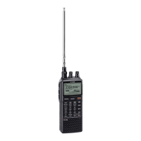
VHF/UHF RF and mixer circuits
30.0-1
999.9999a
MHz
CONV unit
30.0-989.99999
MHz
—
10 de
ATT
RF-B unit
^
~
^BPF2^
-
^BPF3^
¥
BPF4/
Convertor LO
signal
IC3
r^h
Bu^
-6<^
1st LO signal
2nd LO signal
•
MIX unit
778.7
MHz
iC2
266.7 MHz
-<8>
10.7 MHz
to
MAIN
unit
4-1