and
consists of a PLL
1C,
VCO-B
and loop filter
circuits, etc.
The output signal is applied to the 2nd mixer circuit In
the
RF-A or RF-B unit as
a 2nd LO
signal via the
multiplier
circuit.
The generated signal from the VCO-B (VCO-B board,
Q1,
03)
is
amplified
at
the buffer-amplifier
(IC12) and
is then
applied to the
prescaler section In
the PLL
1C
(IC10,
pin
11).
The reference signal from the divider circuit (IC11; 15.1
MHz) is divided at the
programmable divider
section in the
PLL
1C.
The output
signals from
these
section
are phase
detected
at
the phase
detector section,
and then output
from pin
6
of the PLL
1C
via the charge
pump
section.
The output signals
are applied
to the
loop
filter circuit
(Q14,
Q15)
to
converted into DC.
The
DC
voltage
is
then applied
to the
VCO-B circuit.
•
VCO-B output
frequency
Receive freq. [MHz]
VCO-B output Ireq.
{MHz]
VCO
Multiplier
action
0.1-
29.99998
304.8
Q1 i;e
30.0-
489.99999 768.0
Q3
-
500.0-1199.99989 256.0
Q1
-
1200.0-1499.99999 768.0
Q3
-
1500.0-1999.99999
256.0 Q1
-
4-2-3
CONVERTOR
PLL CIRCUIT
(CONV UNIT)
The
generated
signal from
the
convertor
VCO circuit (IC6)
is
amplified
at the buffer-amplifier circuit (IC7) and
then
applied to the PLL IC (IC4) via the low-pass filter circuit
(L29, L30.
C78-C78).
The filtered signal
is
applied
to the
prescaler section to produce an
approx.
100
kHz phase
signal. The reference signal
from the PLL unit
(15.1
MHz)
is divided
at
the programmable
divider
section
in the
PLL
IC, and the phase signals are applied
to the
phase detector
section.
The output signals from
the phase detector section are
applied to the
convertor
VCO circuit
(1C6).
•
Convertor
VCO
output
frequency
Receive freq. [MHz]
Convertor VCO output freq.
[MHz]
Divider
action
1025.0-1199.99999
1000.0 1/2
1200.0-1889.99989
1000.0
bypassed
1990.0-1999.99989
1010.0
bypassed
•
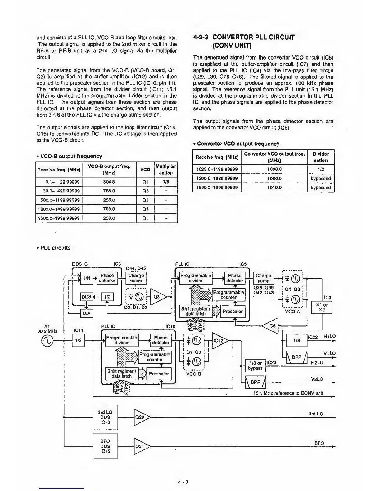
PLL circuits
DOSIC IC3 PLLIC ICS
4-7