4 - 3
• FREQUENCY SYNTHESIZER CIRCUITS
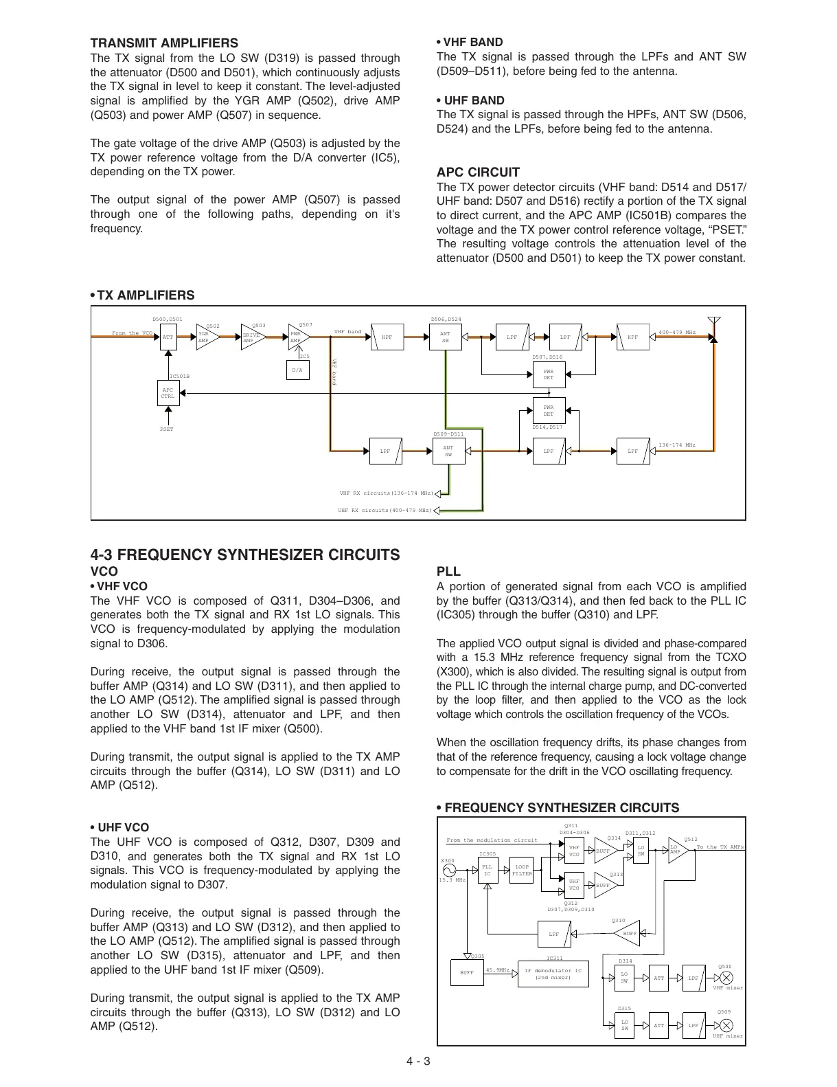
TRANSMIT AMPLIFIERS
The TX signal from the LO SW (D319) is passed through
the attenuator (D500 and D501), which continuously adjusts
the TX signal in level to keep it constant. The level-adjusted
signal is amplified by the YGR AMP (Q502), drive AMP
(Q503) and power AMP (Q507) in sequence.
The gate voltage of the drive AMP (Q503) is adjusted by the
TX power reference voltage from the D/A converter (IC5),
depending on the TX power.
The output signal of the power AMP (Q507) is passed
through one of the following paths, depending on it's
frequency.
ATT
YGR
AMP
PWR
AMP
LPF
ANT
SW
APC
CTRL
ANT
SW
DRIVE
AMP
LPF
HPFHPF LPFLPF
PWR
DET
PWR
DET
LPF
From the VCO
136-174 MHz
D507,D516
D514,D517
Q507
Q503
Q502
D500,D501
IC501B
VHF RX circuits(136-174 MHz)
UHF band
VHF band
UHF RX circuits(400-479 MHz)
D509-D511
D506,D524
PSET
400-479 MHz
D/A
IC5
• TX AMPLIFIERS
BUFF
UHF
VCO
LPF
BUFF
PLL
IC
LO
AMP
FILTER
LOOP
VHF
VCO
ATT
ATT
LPF
LPF
BUFF
UHF mixer
VHF mixer
From the modulation circuit
IF demodulator IC
(2nd mixer)
15.3 MHz
45.9MHz
Q512
To the TX AMPs
IC305
X300
Q509
Q500
Q305
IC311
LO
SW
LO
SW
D304-D306
Q311
Q314
Q313
D307,D309,D310
Q312
D311,D312
Q310
D314
D315
LO
SW
BUFF
4-3
FREQUENCY SYNTHESIZER CIRCUITS
VCO
• VHF VCO
The VHF VCO is composed of Q311, D304–D306, and
generates both the TX signal and RX 1st LO signals. This
VCO is frequency-modulated by applying the modulation
signal to D306.
During receive, the output signal is passed through the
buffer AMP (Q314) and LO SW (D311), and then applied to
the LO AMP (Q512). The amplified signal is passed through
another LO SW (D314), attenuator and LPF, and then
applied to the VHF band 1st IF mixer (Q500).
During transmit, the output signal is applied to the TX AMP
circuits through the buffer (Q314), LO SW (D311) and LO
AMP (Q512).
• UHF VCO
The UHF VCO is composed of Q312, D307, D309 and
D310
, and generates both the TX signal and RX 1st LO
signals
. This VCO is frequency-modulated by applying the
modulation signal to D307.
During receive, the output signal is passed through the
buffer AMP (Q313) and LO SW (D312), and then applied to
the LO AMP (Q512). The amplified signal is passed through
another LO SW (D315), attenuator and LPF, and then
applied to the UHF band 1st IF mixer (Q509).
During transmit, the output signal is applied to the TX AMP
circuits through the buffer (Q313), LO SW (D312) and LO
AMP (Q512).
• VHF BAND
The TX signal is passed through the LPFs and ANT SW
(D509–D511), before being fed to the antenna.
• UHF BAND
The TX signal is passed through the HPFs, ANT SW (D506,
D524) and the LPFs, before being fed to the antenna.
APC CIRCUIT
The TX power detector circuits (VHF band: D514 and D517/
UHF band: D507 and D516) rectify a portion of the TX signal
to direct current, and the APC AMP (IC501B) compares the
voltage and the TX power control reference voltage, “PSET.”
The resulting voltage controls the attenuation level of the
attenuator (D500 and D501) to keep the TX power constant.
PLL
A portion of generated signal from each VCO is amplified
by the buffer (Q313/Q314), and then fed back to the PLL IC
(IC305) through the buffer (Q310) and LPF.
The applied VCO output signal is divided and phase-compared
with a 15.3 MHz reference frequency signal from the TCXO
(X300), which is also divided. The resulting signal is output from
the PLL IC through the internal charge pump, and DC-converted
by the loop filter, and then applied to the VCO as the lock
voltage which controls the oscillation frequency of the VCOs.
When the oscillation frequency drifts, its phase changes from
that of the reference frequency, causing a lock voltage change
to compensate for the drift in the VCO oscillating frequency.
 Loading...