Do you have a question about the Icom IC-V200T and is the answer not in the manual?
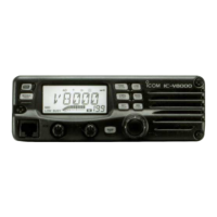
General specifications including frequency coverage, emission type, and dimensions.
Transmitter specifications such as output power, modulation, and deviation.
Receiver specifications like sensitivity, selectivity, and audio output.
Internal layout and component identification for the main unit.
Internal layout and component identification for the logic unit.
Detailed explanation of receiver circuit functions and signal paths.
Detailed explanation of transmitter circuit functions and signal paths.
Description of Phase-Locked Loop circuits, frequency generation, and control.
Explanation of CPU, memory, and peripheral circuits in the logic unit.
Description of the 5-tone encoder/decoder IC and related functions.
Explanation of the LCD controller and display indicators.
List of front panel and chassis components with order numbers.
List of optional accessories and their part numbers.
Comprehensive list of parts for the main unit.
Comprehensive list of parts for the logic unit.
Required test equipment and connection setup for servicing.
Procedures for adjusting PLL reference frequency and lock voltage.
Steps for adjusting receiver sensitivity and squelch.
Procedures for adjusting transmitter output power and deviation.
Component layout diagrams for front, VR, and CTCSS units.
Component layout diagram for the logic unit.
Component layout diagram for the main unit.
| Frequency Range | 144-148 MHz |
|---|---|
| Modulation Type | FM |
| Antenna Impedance | 50 Ω |
| Voltage | 13.8 V |
| Current Consumption (Transmit) | 1.5 A |
| Power Output | 5.0 W (High), 0.5 W (Low) |
| Supply voltage | 13.8 V DC ±15% |