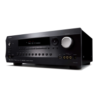
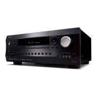
DTR-6.5
IC BLOCK DIAGRAMS AND DESCRIPTIONS
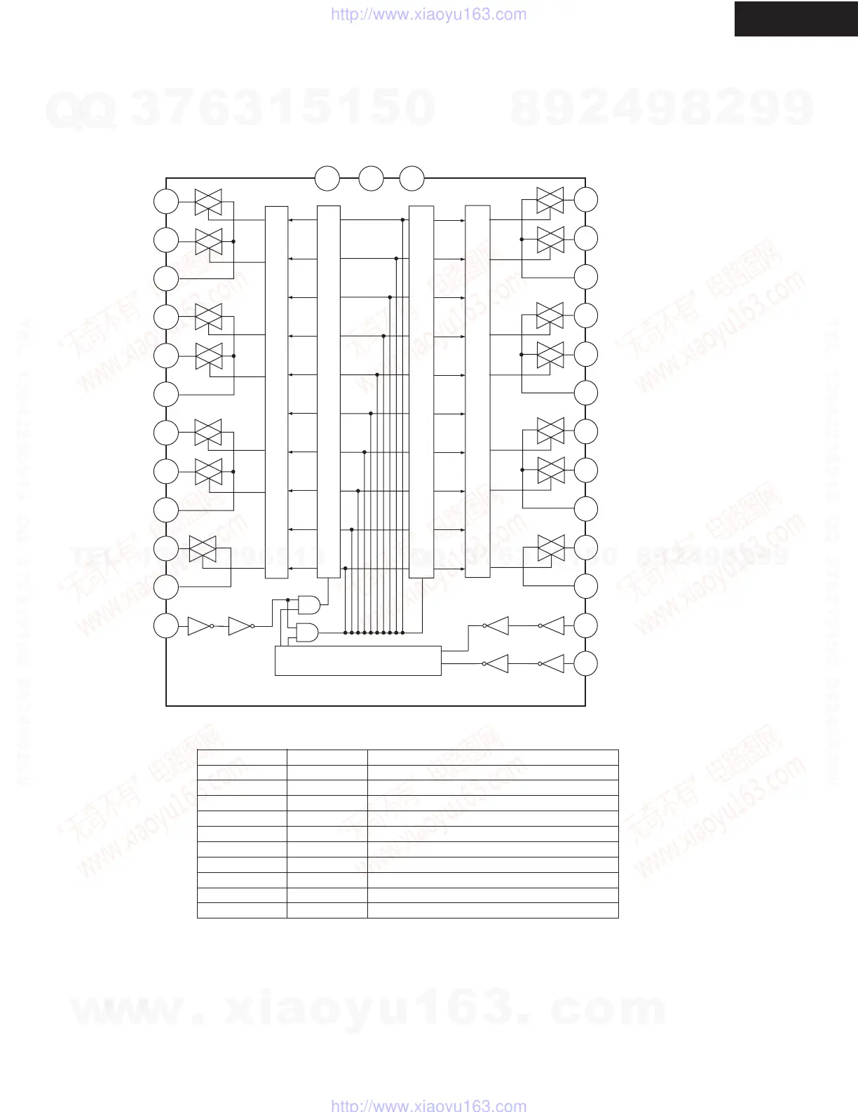
TC9162BFG(Function Switch)
2
3
4
5
6
7
8
9
10
11
12
13
15
16
17
18
19
20
21
22
23
24
25
26
27
28
14
1
VSS GND VDD
S1
S2
S3
COM1
S4
S5
S6
COM2
S7
COM4
ST
DATA
CK
LEVEL SHIFT
LATCH CIRCUIT
SHIFT REGISTER
LATCH CIRCUIT
LEVEL SHIFT
COM3
S1
S2
S3
COM1
S4
S5
S6
COM2
S7
COM4
COM3
1
14
28
2,3,5,6,8,9,11
27,26,24,23,21,20,18
4,7,10,12
25,22,19,17
13
15
16
Symbol
GND
VDD
S1~S7
S1~S7
COM1~COM4
COM1~COM4
ST
CK
DAT
A
Pin No. Function
Negative power supply
Ground
Positive power supply
Input/output terminals
Input/output terminals
Common terminals
Common terminals
Strobe input terminal for data reading
Clock input terminal for data transfer
Data input terminal for switch
Vss
w
w
w
.
x
i
a
o
y
u
1
6
3
.
c
o
m
Q
Q
3
7
6
3
1
5
1
5
0
9
9
2
8
9
4
2
9
8
T
E
L
1
3
9
4
2
2
9
6
5
1
3
9
9
2
8
9
4
2
9
8
0
5
1
5
1
3
6
7
3
Q
Q
TEL 13942296513 QQ 376315150 892498299
TEL 13942296513 QQ 376315150 892498299
http://www.xiaoyu163.com
http://www.xiaoyu163.com