34 Datasheet
Electrical Specifications
2.13 GTL+ FSB Specifications
Termination resistors are not required for most GTL+ signals, as these are integrated into the
processor silicon.Valid high and low levels are determined by the input buffers which compare a
signal’s voltage with a reference voltage called GTLREF. Table 2-18 lists the GTLREF
specifications. The GTL+ reference voltage (GTLREF) should be generated on the system board
using high precision voltage divider circuits.
§
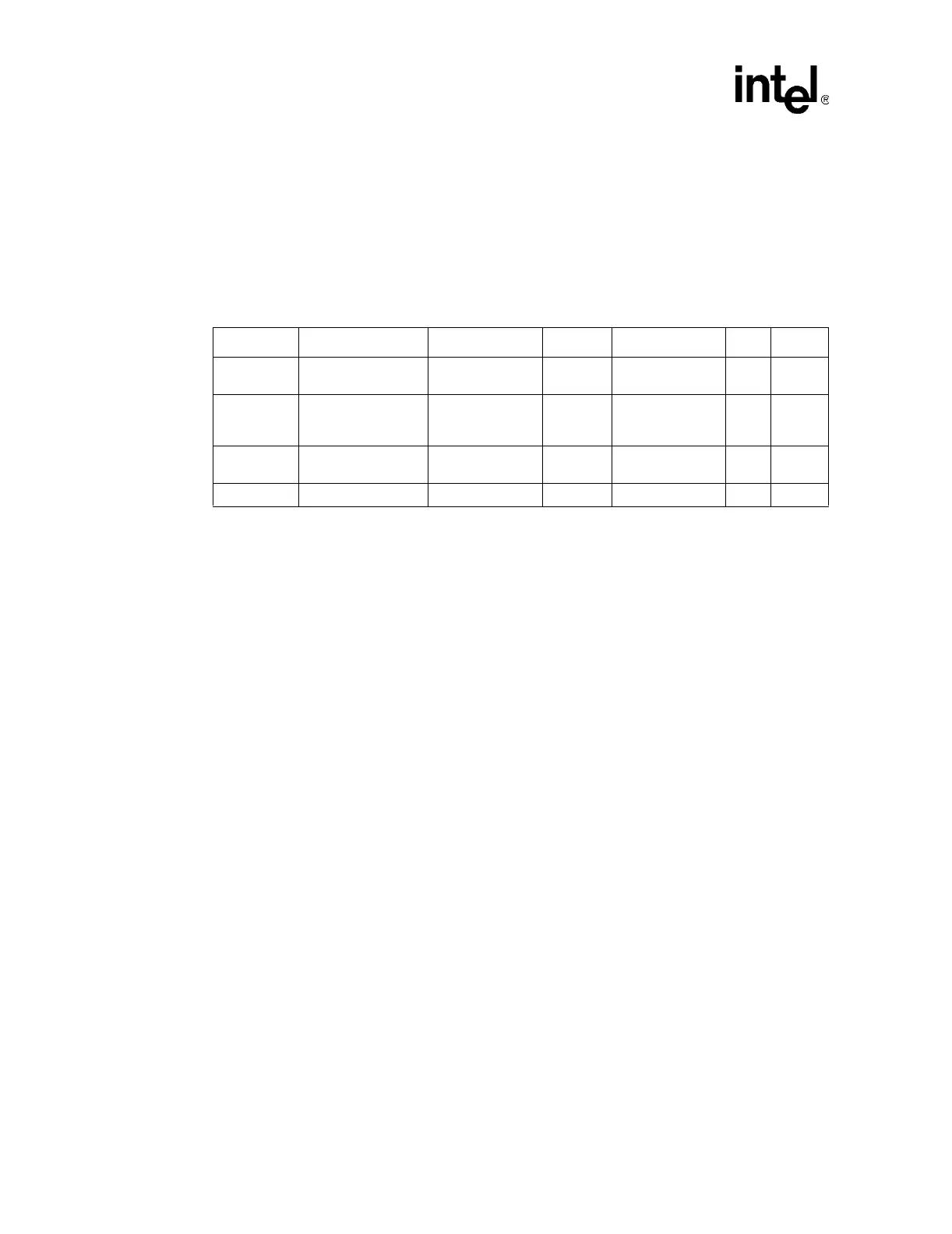
Table 2-18. GTL+ Bus Voltage Definitions
Symbol Parameter Min Typ Max Units Notes
1
NOTES:
1. Unless otherwise noted, all specifications in this table apply to all processor frequencies.
GTLREF
Bus Reference
Voltage
(0.98 * 0.67) * V
TT
0.67 * V
TT
(1.02 * 0.67) * V
TT
V
2, 3, 4,
5
2. The tolerances for this specification have been stated generically to enable the system designer to calculate the minimum
and maximum values across the range of V
TT
.
3. GTLREF should be generated from V
TT
by a voltage divider of 1% resistors or 1% matched resistors.
4. The V
TT
referred to in these specifications is the instantaneous V
TT
.
5. The Intel
®
915G/915GV/915P and 910GL Express chipset platforms use a pull-up resistor of 100 Ω and a pull-down resistor
of 210 Ω. Contact your Intel representative for further details and documentation.
R
PULLUP
On die pullup for
BOOTSELECT
signal
500 — 5000 Ω
6
6. These pull-ups are to V
TT
.
R
TT
Termination
Resistance
54 60 66 Ω
7
7. R
TT
is the on-die termination resistance measured at V
TT
/2 of the GTL+ output driver.
COMP[1:0] COMP Resistance 59.8 60.4 61 Ω
8
8. COMP resistance must be provided on the system board with 1% resistors. COMP[1:0] resistors are to V
SS
.
 Loading...