High-Level Functional Description
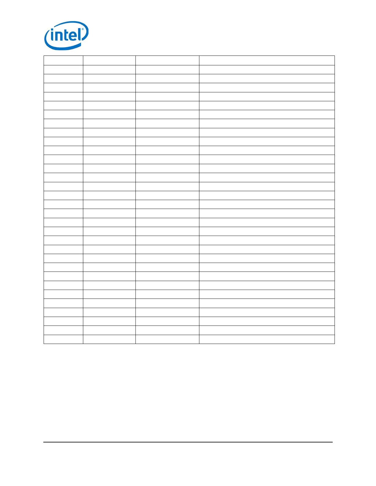
Pin Description
J18 - pin 12 GP129 UART1_RTS GPIO, UART1 ready to send output.
J18 - pin 13 GP130 UART1_RX GPIO, UART1 receive data input.
J18 - pin 14 FW_RCVR Firmware recovery, active high on boot.
J20 - pin 1 V_VSYS System input power.
J20 - pin 2 V_V3P30 System 3.3 V output.
J20 - pin 3 GP134 UART2_RX UART2 Rx (input).
J20 - pin 4 GP45 COMPASS_DRDY GPIO, compass data ready input.
J20 - pin 5 GP47 ACCELEROMETER_INT_2 GPIO, accelerometer interrupt input 2.
J20 - pin 6 GP49 GYRO_INT GPIO, gyro interrupt input.
J20 - pin 7 GP15 GPIO.
J20 - pin 8 GP84 SD_CLK_FB GPIO, SD clock feedback input.
J20 - pin 9 GP42 SSP2_RXD GPIO, SSP2 Rx data input.
J20 - pin 10 GP41 SSP2_FS GPIO, SSP2 frame sync output.
J20 - pin 11 GP78 SD_CLK GPIO, SD clock output.
J20 - pin 12 GP79 SD_CMD GPIO, SD command.
J20 - pin 13 GP80 SD_DAT0 GPIO, SD data 0.
J20 - pin 14 GP81 SD_DAT1 GP81 SD data 1.
J19 - pin 1 NC No connect.
J19 - pin 2 V_V1P80 System 1.8 V I/O output power.
J19 - pin 3 GND Ground.
J19 - pin 4 GP44 ALS_INT_N GPIO, ALS interrupt input.
J19 - pin 5 GP46 ACCELEROMETER_INT_1 GPIO, accelerometer interrupt input.
J19 - pin 6 GP48 GYRO_DRDY GPIO, gyro data ready input.
J19 - pin 7 RESET_OUT# System reset out low.
J19 - pin 8 GP131 UART1_TX GPIO, UART 1 Tx output.
J19 - pin 9 GP14 AUDIO_CODEC_INT GPIO, audio codec interrupt input.
J19 - pin 10 GP40 SSP2_CLK GPIO, SSP2 clock output.
J19 - pin 11 GP43 SSP2_TXD GPIO, SSP2 transmit data output.
J19 - pin 12 GP77 SD_CDN GPIO, SD card detect low input.
J19 - pin 13 GP82 SD_DAT2 GPIO, SD data 2
J19 - pin 14 GP83 SD_DAT3 GPIO, SD data 3
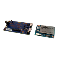
2.3 Intel® Edison Breakout Board expansion power supply
Intel® Edison is a low-power device. In general, it does not draw more than 200 mA with 600 mA short duration
spikes during Wi-Fi transmit. Therefore, an Intel® Edison device may run on USB power (when configured as a
device), or an external power adapter from 7 to 15 V.
Power from the external power adapter goes to a DC-DC converter and down-converted to 5 V. The 5 V rail is
diode ORed with the USB VBUS rail. This power goes to a battery recharger IC, which limits the output voltage to
4.4 V. This voltage is in the safe range for the Edison module VSYS. The VSYS power range is 3.15 to 4.5 V. This
allows the Intel® Edison device to run off a standard lithium-ion battery. The charger IC is configured to limit the
current to 1 A. The charger is programmed to charge at 190 mA. This charger is designed to charge standard
lithium-ion batteries with 4.2 V maximum charging voltage. You are responsible for choosing a suitable battery and
following all safety precautions, to prevent overcharging or charging when the battery temperature is too high.
Intel® Edison Breakout Board
Hardware Guide January 2015
10 Document Number: 331190-006