High-Level Functional Description
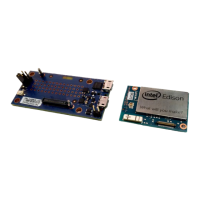
2.2 Intel® Edison Breakout Board expansion header
This section explains the expansion header.
When the pin mode is chosen as GPIO, it can be programmed as an output or input. When programmed as an input,
a GPIO can serve as an interrupt or wake source. Inputs have programmable pullups or pulldowns. Pullup value can
be 2, 20, or 50 kohm. I2C pins also have an additional 910 ohm value.
When in general purpose mode, input GPIO signals enter a glitch filter by default, before reaching the edge
detection registers. To ensure that a pulse is detected by the edge detection register, the pulse should be five clock
cycles long.
• 100 ns for a 50 MHz clock when SoC is in S0 state.
• 260 ns for 19.2 MHz clock when SoC is in S0i1 or S0i2 State.
• 155.5 µs for 32 kHz clock (RTC) when SoC is in S0i3 State.
Most GPIO capable pins are configured as GPIO inputs during the assertion of all resets and they remain inputs
until configured otherwise.
As outputs, the GPIOs can be individually cleared or set. They can be pre-programmed to either state when
entering standby. Output drive is ±3 mA.
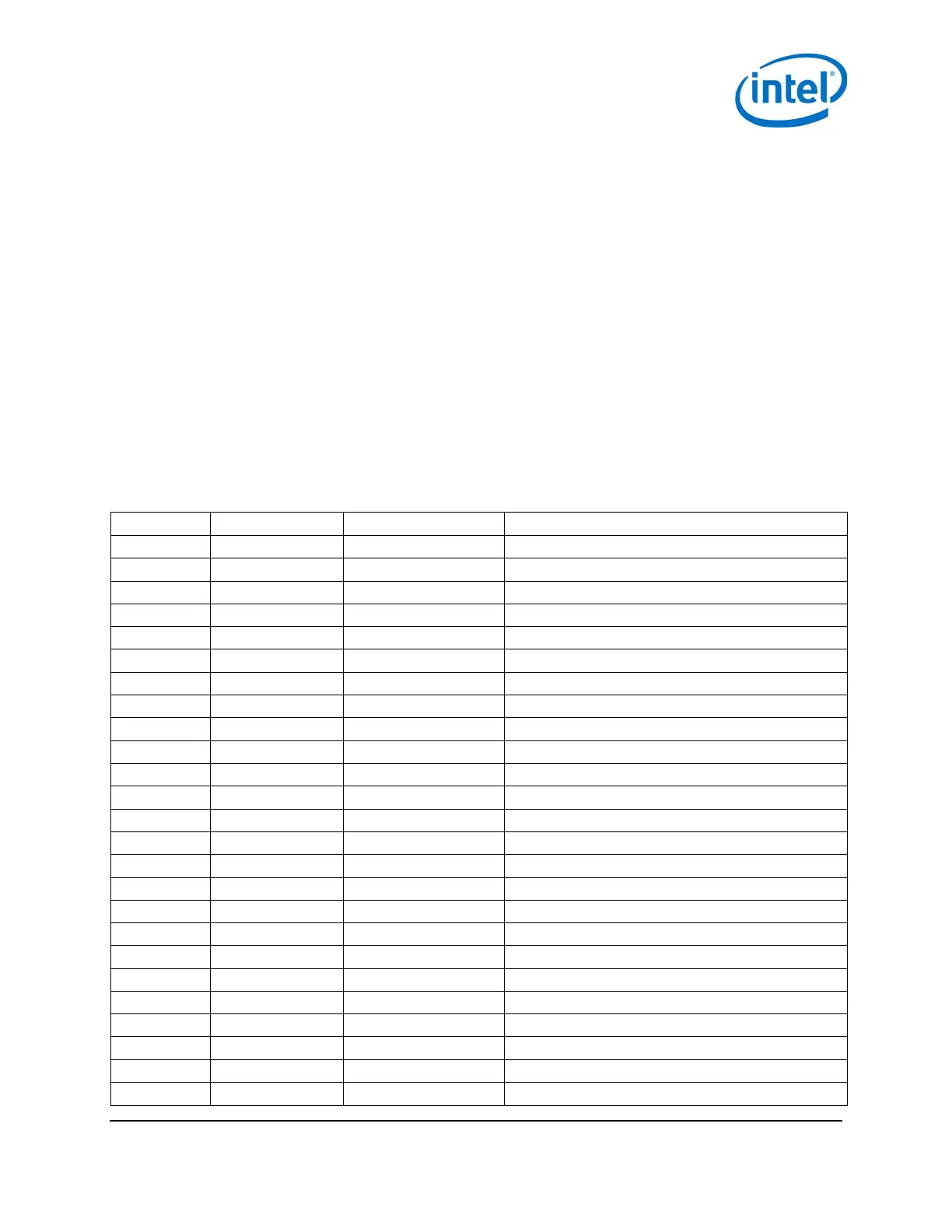
Table 2 Intel® Edison breakout board expansion header signal list
Pin Description
J17 - pin 1 GP182_PWM2 GPIO capable of PWM output.
J17 - pin 2 NC No connect.
J17 - pin 3 NC No connect.
J17 - pin 4 VIN 7 to 15 V.
J17 - pin 5 GP135 UART2_TX GPIO, UART2 transmit output.
J17 - pin 6 RCVR_MODE Firmware recovery mode.
J17 - pin 7 GP27 I2C6_SCL GPIO,IC26 SCL output open collector.
J17 - pin 8 GP20 I2C1_SDA GPIO, I2C1 data open collector.
J17 - pin 9 GP28 I2C6_SDA GPIO, I2C6 data open collector.
J17 - pin 10 GP111 SSP5_FS1 GPIO, SSP2 chip select 2 output.
J17 - pin 11 GP109 SSP5_CLK GPIO, SSP5 clock output.
J17 - pin 12 GP115 SSP5_TXD GPIO, SSP5 transmit data output.
J17 - pin 13 OSC_CLK_OUT_0 High speed clock output.
J17 - pin 14 GP128 UART1_CTS GPIO, UART1 clear to send input.
J18 - pin 1 GP13_PWM1 GPIO capable of PWM output.
J18 - pin 2 GP165 GPIO
J18 - pin 3 GPI_PWRBTN_N Power button input.
J18 - pin 4 MSIC_SLP_CLK2 32 kHz sleep clock.
J18 - pin 5 V_VBAT_BKUP RTC backup battery input.
J18 - pin 6 GP19 I2C1_SCL GPIO,IC21 SCL output open collector.
J18 - pin 7 GP12_PWM0 GPIO capable of PWM output.
J18 - pin 8 GP183_PWM3 GPIO capable of PWM output.
J18 - pin 9 NC No connect.
J18 - pin 10 GP110 SSP5_FS0 GPIO, SSP1 chip select 2 output.
J18 - pin 11 GP114 SSP5_RX GPIO, SSP5 receive data input.
Intel® Edison Breakout Board
January 2015 Hardware Guide
Document Number: 331190-006 9