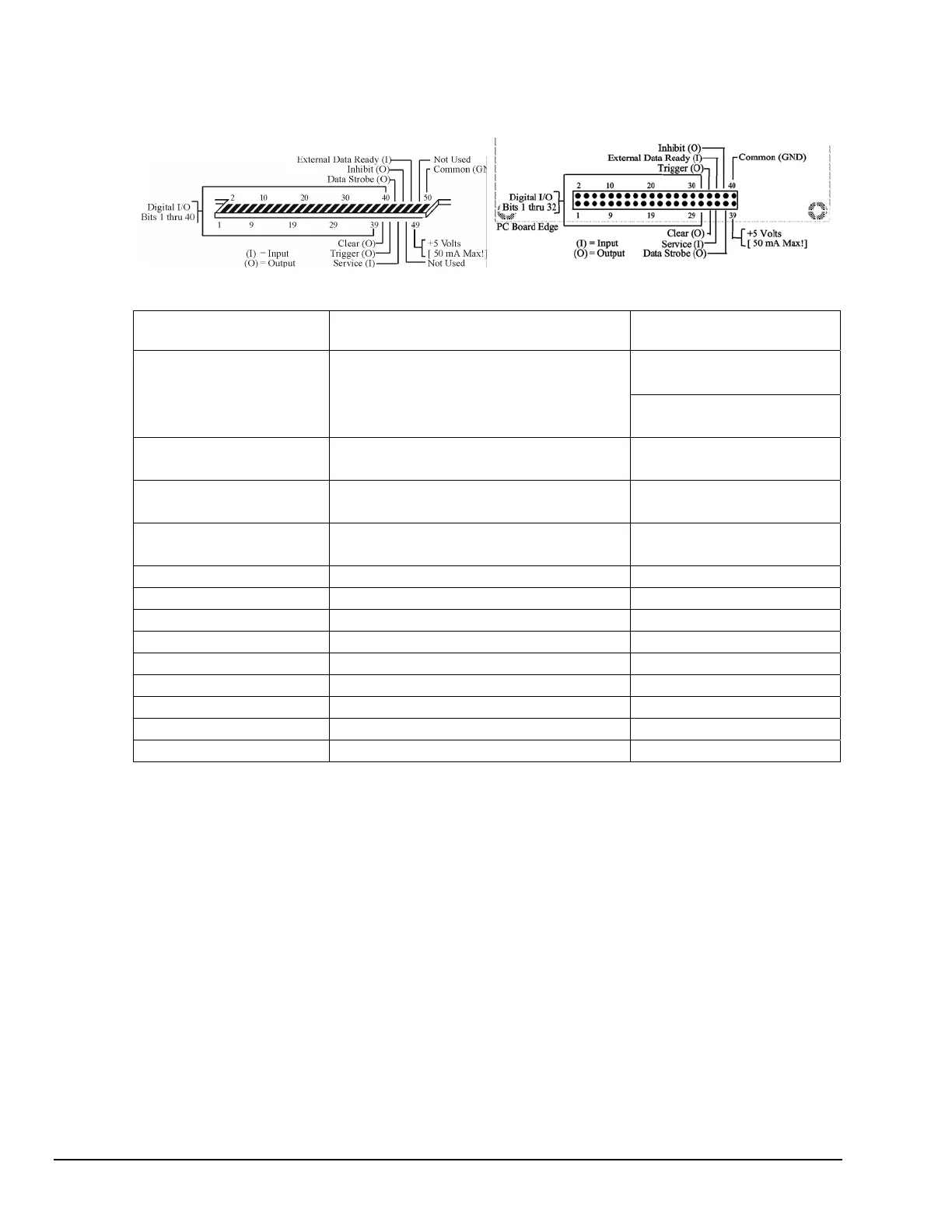
Digital I/O Port Pin Outs
The following diagram illustrates the digital I/O edge connector as view from the rear of the Digital488 and
the top PC Board edge view of the Digital488/32/OEM.
Digital488 Rear Panel I/O Connector Pin Out Digital488/32/OEM I/O Connector Pin Out
Pin
Digital488
Description
Pin
Digital488/32/OEM
1 thru 8
Least Significant Port
DATA PORT1 (Input or Output).
Pin 1 is bit 1 (LSB), Pin 8 is bit 8 (MSB).
1 thru 8
Least Significant Port
9 thru 16
DATA PORT2 (Input or Output)
Pin 9 is bit 1 (LSB), Pin 16 is bit 8 (MSB)
9 thru 16
17 thru 24
DATA PORT3 (Input or Output)
Pin 17 is bit 1 (LSB), Pin 24 is bit 8 (MSB)
17 thru 24
25 thru 32
DATA PORT4 (Input or Output)
Pin 25 is bit 1 (LSB), Pin 32 is bit 8 (MSB)
25 thru 32
Most Significant Port
33 thru 40
Most Significant Port
DATA PORT5 (Input or Output
Pin 33 is bit 1 (LSB), Pin 40 is bit 8 (MSB)
N/A
41 CLEAR (Output) 33
42 DATA STROBE (Output) 37
43 TRIGGER (Output) 34
44 INHIBIT (Output) 38
45 SERVICE INPUT (Input). 35
46 EXTERNAL DATA READY [EDR] (Input) 36
47,48 Not used N/A
49 +5 Volts (Do not exceed 50 mA load) 39
50 I/O COMMON (Gnd) 40
2-4, Getting Started 11-19-01 Digital488 User’s Manual