© 2017 Jackson Labs Technologies, Inc. 5
Mini-JLT GNSS™ User Manual
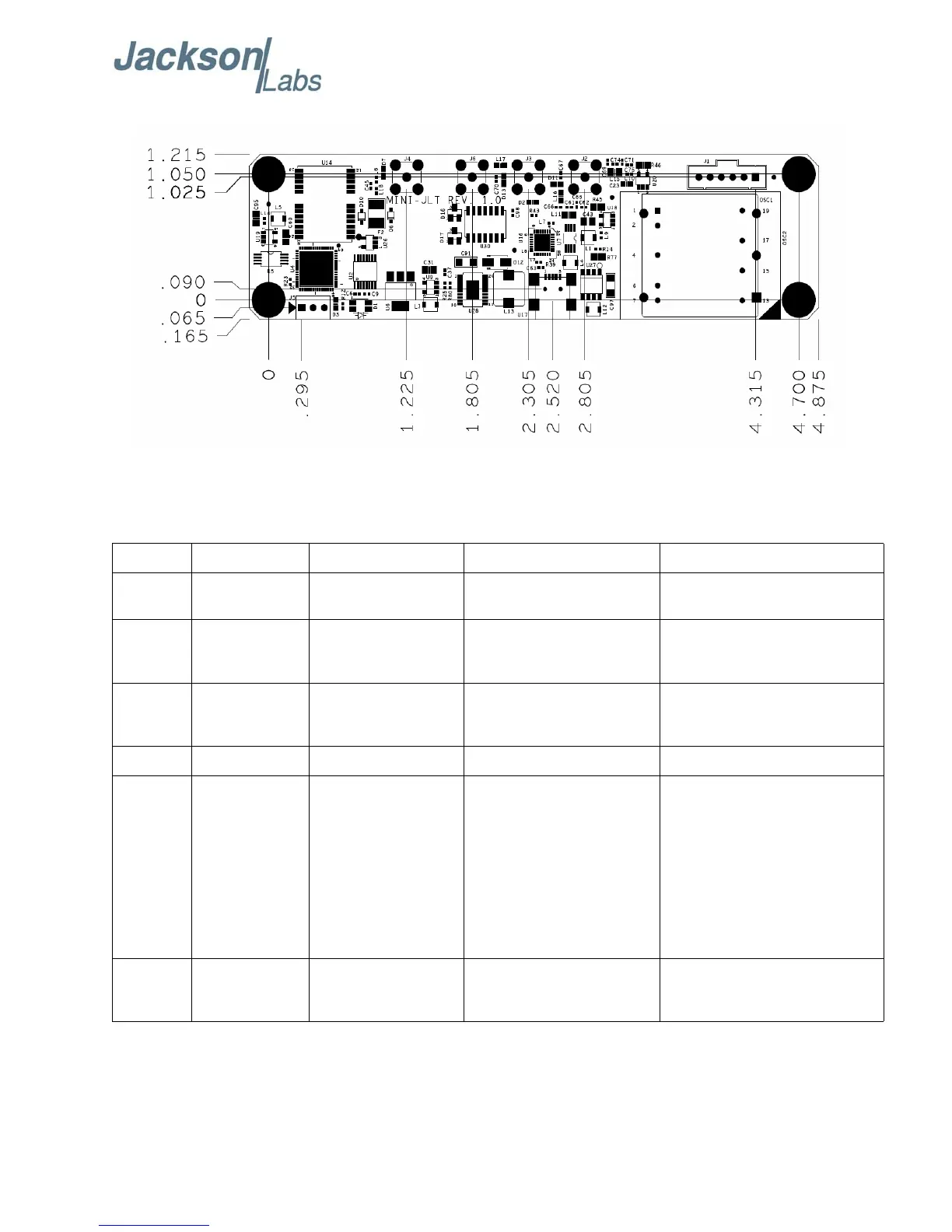
Figure 2.2 Mini-JLT GNSS™ Mechanical Dimensions
Table 2.1shows the Mini-JLT GNSS™ revision 1.0 hardware pin descriptions
Table 2.1 Mini-JLT GNSS™ hardware connectors
Ref Name Function
Specification
Description
J1 Pin 1 1PPS In Optional external 1PPS
Input
0V to 5V, pulled-low by 4.7K
resistor
Alternate 1PPS reference input
J1 Pin 2 Serial TX Serial Transmit Output 3.3V LVCMOS (RS-232 serial
optional)
Serial Transmit output for NMEA and
SCPI sentences, internally
connected to USB TX signal
J1 Pin 3 Serial RX Serial Receive Input 3.3V LVCMOS (RS-232 serial
optional), 5V compatible.
Serial Receive input for SCPI
commands, internally wired-ored to
USB RX signal
J1 Pin 4 Ground Ground Ground Main Power Return
J1 Pin 5 VANT External Antenna
Voltage
3.0V to 5.5V up to 100mA The unit provides a 3.3V antenna
supply to the GNSS antenna by
default. This can be over-driven by a
voltage >3.3V supplied to the VANT
pin. Both the internal 3.3V and the
external VANT supply are diode-ored
and protected against each other.
The VANT current is fused by a
100mA self-resetting fuse on the
PCB.
J1 Pin 6 +5V Power Main Power Supply 4.0V to 6.0V range, 5V nominal Supplies power to the unit and the
OCXO. Up to 8W are required during
warmup. Range is 5V +/-1.0V
 Loading...