61
7 Modbus address tables
7.2.4 Ramp slope, controllers 1, 2
7.2.5 Controller 1, parameter block 1
7.2.6 Controller 1, parameter block 2
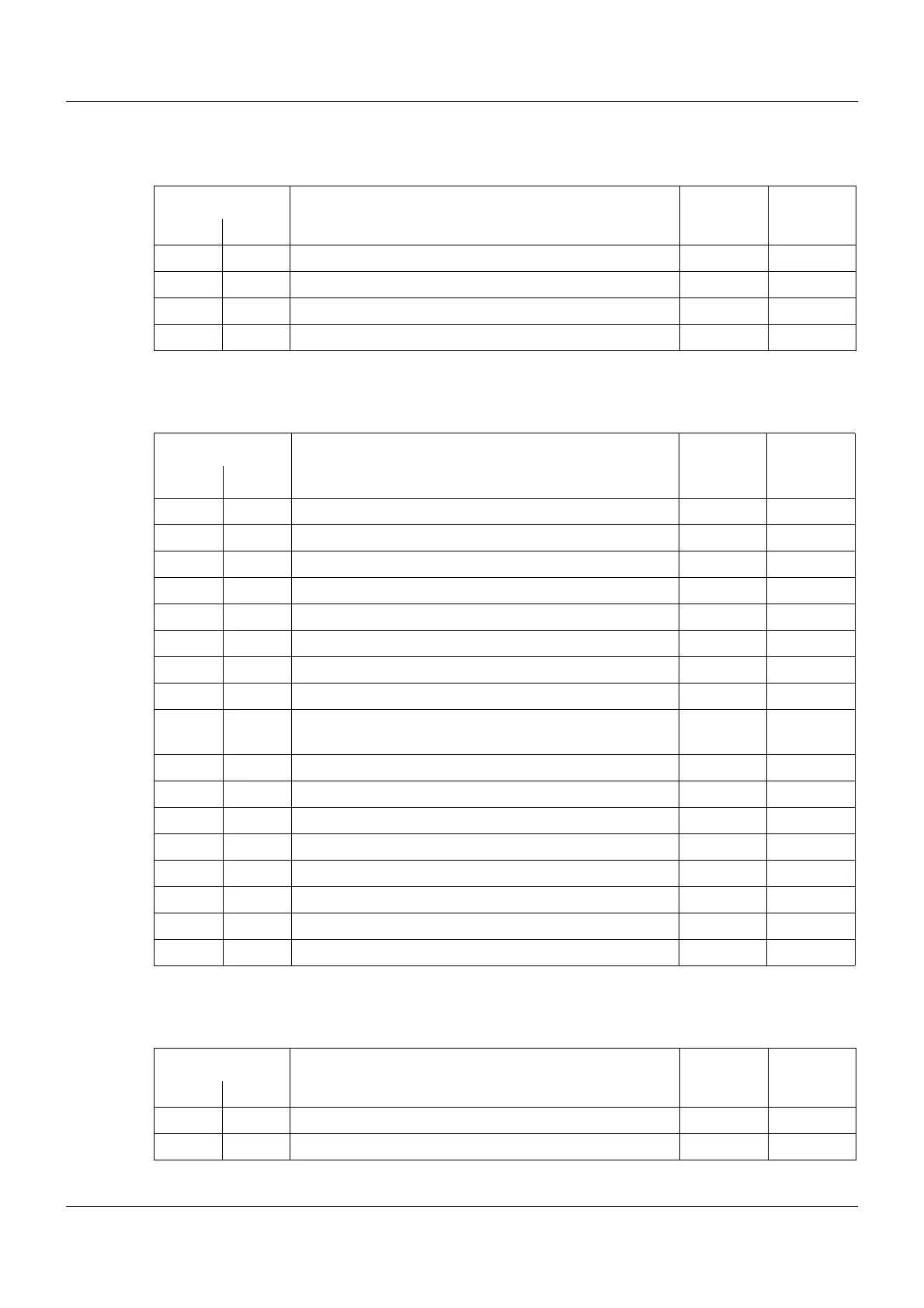
Modbus address Signal designation Data type Access
Hex. Dec.
0x1091 4241 Ramp slope for positive gradient, controller 1 FLOAT R/W
0x1093 4243 Ramp slope for negative gradient, controller 1 FLOAT R/W
0x1095 4245 Ramp slope for positive gradient, controller 2 FLOAT R/W
0x1097 4247 Ramp slope for negative gradient, controller 2 FLOAT R/W
Modbus address Signal designation Data type Access
Hex. Dec.
0x1099 4249 XP1 proportional band (P component) FLOAT R/W
0x109B 4251 XP2 proportional band (P component) FLOAT R/W
0x109D 4253 TV1 derivative time (D component) FLOAT R/W
0x109F 4255 TV2 derivative time (D component) FLOAT R/W
0x10A1 4257 TN1 reset time (I component) FLOAT R/W
0x10A3 4259 TN2 reset time (I component) FLOAT R/W
0x10A5 4261 CY1 cycle time FLOAT R/W
0x10A7 4263 CY2 cycle time FLOAT R/W
0x10A9 4265 XSH switching hysteresis between 1st and 2nd digital
output
FLOAT R/W
0x10AB 4267 XD1 switching differential of the 1st digital output FLOAT R/W
0x10AD 4269 XD2 switching differential of the 2nd digital output FLOAT R/W
0x10AF 4271 TT actuator time INT16 R/W
0x10B0 4272 Y0 working point INT16 R/W
0x10B1 4273 Y1 output value limit INT16 R/W
0x10B2 4274 Y2 output value limit INT16 R/W
0x10B3 4275 TK1 minimum start time of the 1st digital output FLOAT R/W
0x10B5 4277 TK2 minimum start time of the 2nd digital output FLOAT R/W
Modbus address Signal designation Data type Access
Hex. Dec.
0x10B7 4279 XP1 proportional band (P component) FLOAT R/W
0x10B9 4281 XP2 proportional band (P component) FLOAT R/W
 Loading...


