(No.49837)1-29
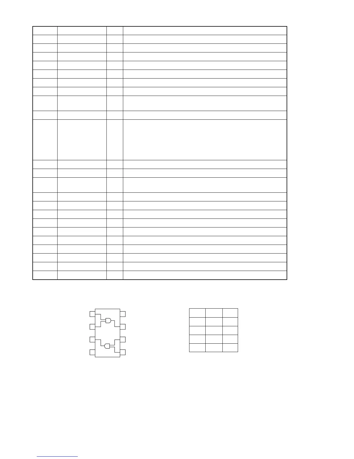
4.3 TC7W08FU-X (IC107) : Nand gate
• Pin layout & Block diagram • Truth table
63 LWR# O RISC interface write enable (active-low).
64 LOE# O RISC interface output enable (active-low).
65~67 LCS[3,1,0]# O RISC interface chip select (active-low).
68~79 LA[0:17] O RISC interface address.
80 VSS I Ground.
81 VPP I 5.0V power supply.
82~87 LA[0:17] O RISC interface address.
88 ACLK I/O Master clock for external audio DAC (8.192MHz, 11.2896MHz,
12.288MHz, 16.9344MHz, and 18.432MHz).
89 AOUT O Audio interface serial data.
SEL_PLL0 I Used with SEL_PLL1 pin 91 to select phase-lock loop (PLL) clock
frequency of CPUCLK pin 42:
00 = bypass PLL.
01 = 54MHz PLL.
10 = 67.5MHz PLL.
11 = 81MHz PLL.
90 ATCLK I/O Audio transmit bit clock.
91 ATFS O Audio interface transmit frame sync.
SEL_PLL1 I Used with SEL_PLL0 pin 89 to select phase-lock loop (PLL) clock
frequency of CPUCLK pin 42,
92 MA9 O Multiplexed memory row and column address.
DOE# O Memory output enable (active-low).
93 AIN I Audio interface serial data.
94 ARFS I Audio receive bit clock.
95 ARCLK I Audio interface receive frame sync.
96 TDMCLK I TDM serial clock.
97 TDMDR I TDM serial data receive.
98 TDMFS I TDM frame sync.
99 CAS# O Memory colomn address strobe (active-low).
100 VSS I Ground.
Pin No. Symbol I/O Descriptions
Vcc
1Y
2B
2A
1A
1B
2Y
GND
1
2
3
4
8
7
6
5
ABY
LLL
LHL
HLL
HHH
 Loading...