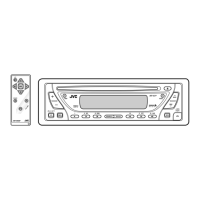
1-38 (No.49837)
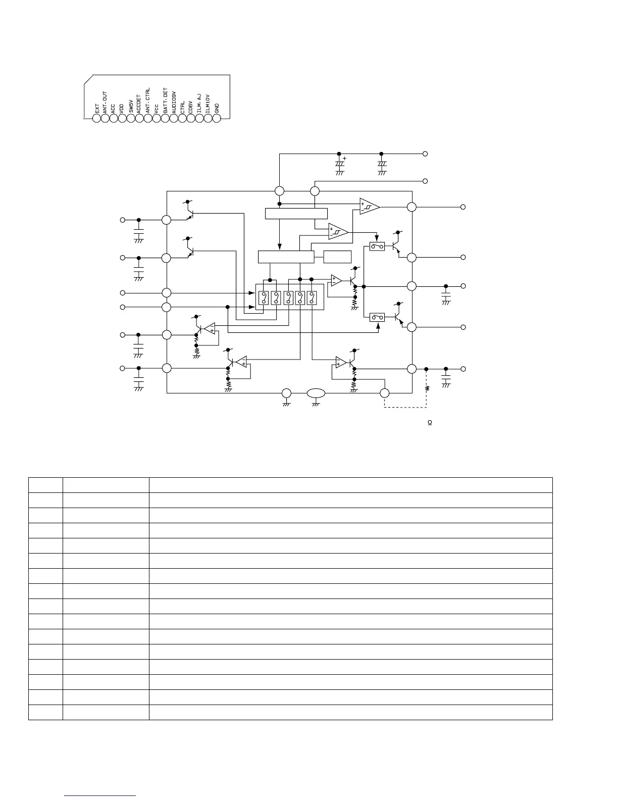
4.12 HA13164A (IC901) : Regulator
• Terminal layout
• Block diagram
• Pin function
123456789101112131415
Pin No. Symbol Function
1 EXTOUT Output voltage is VCC-1 V when M or H level applied to CTRL pin.
2 ANTOUT Output voltage is VCC-1 V when M or H level to CTRL pin and H level to ANT-CTRL.
3 ACCIN Connected to ACC.
4 VDDOUT Regular 5.7V.
5 SW5VOUT Output voltage is 5V when M or H level applied to CTRL pin.
6 COMPOUT Output for ACC detector.
7 ANT CTRL L:ANT output OFF H:ANT output ON
8 VCC Connected to VCC.
9 BATT DET Low battery detect.
10 AUDIO OUT Output voltage is 9V when M or H level applied to CTRL pin.
11 CTRL L:BIAS OFF M:BIAS ON H:CD ON
12 CD OUT Output voltage is 8V when H level applied to CTRL pin.
13 ILM AJ Adjustment pin for ILM output voltage.
14 ILM OUT Output voltage is 10V when M or H level applied to CTRL pin.
15 GND Connected to GND.
2
1
11
12
10
15
13
14
5
4
6
3
8
9
7
ILM AJGND GND
C6
10u
C5
0.1u
C4
0.1u
C3
0.1u
AUDIO OUT
CD OUT
CTRL
ANT CTRL
EXT OUT
ANT OUT
VCC ACC
Surge Protector
BIAS TSD
C1
100u
C2
0.1u
+B
ACC
BATT.DET OUT
COMPOUT
VDD OUT
SW5VOUT
ILMOUT
C7
0.1u
C8
0.1u
R1
UNIT R:
C:F
note1) TAB (header of IC)
connected to GND
TAB
 Loading...