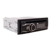
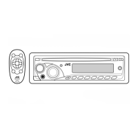
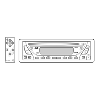
(No.49837)1-33
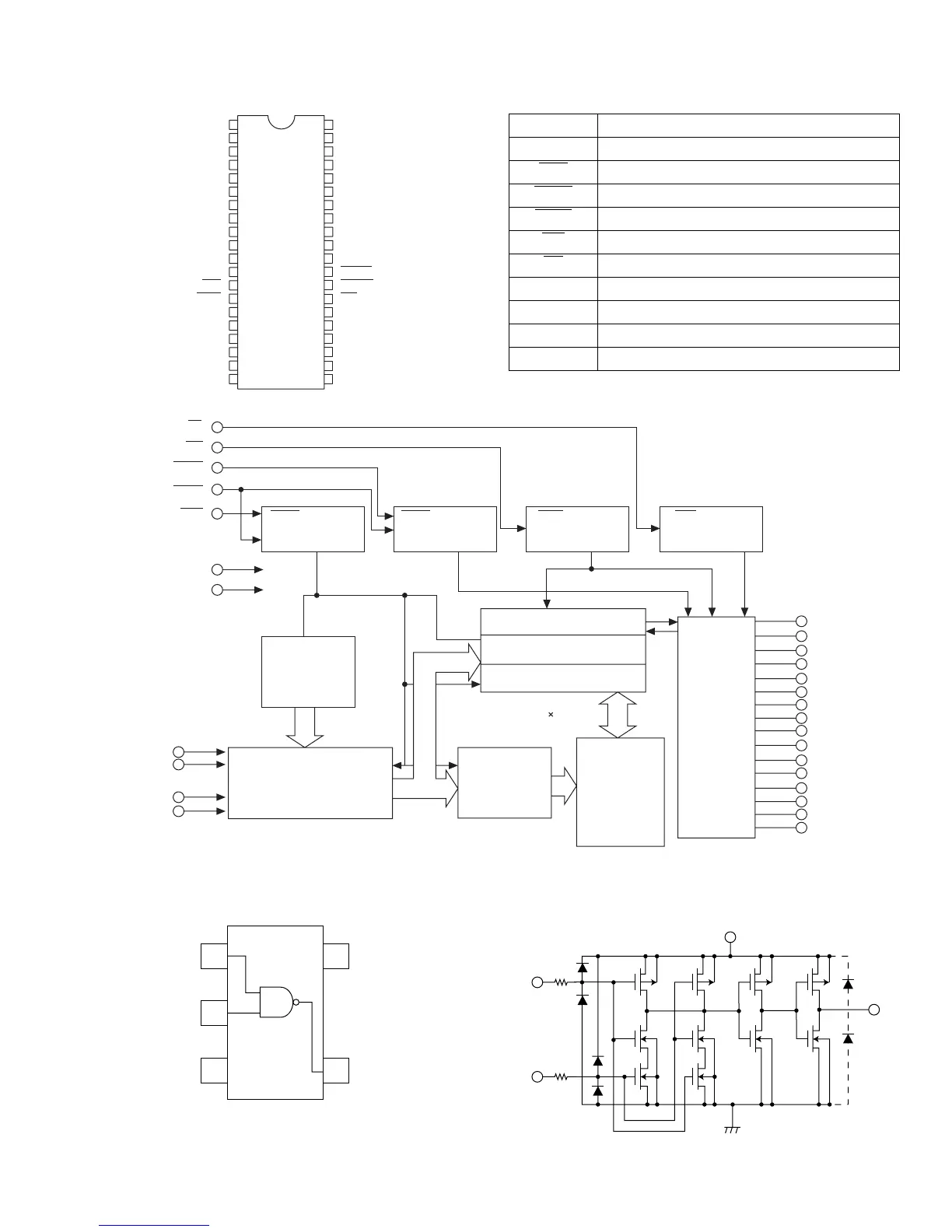
4.6 GLT44016-35J4-X (IC103) : Dram
•Pin layout •Pin function
• Block diagram
4.7 TC7S08F-W (IC106) : Buffer
• Pin layout • Block diagram
1
2
3
4
5
6
7
8
9
10
11
12
13
14
15
16
17
18
19
20
Vcc
DQ
1
DQ2
DQ3
DQ
4
Vcc
DQ
5
DQ
6
DQ
7
DQ
8
NC
NC
WE
RAS
NC
A
0
A1
A2
A3
Vcc
40
39
38
37
36
35
34
33
32
31
30
29
28
27
26
25
24
23
22
21
Vss
DQ
16
DQ
15
DQ
14
DQ
13
Vss
DQ
12
DQ
11
DQ
10
DQ9
NC
LCAS
UCAS
OE
A
8
A
7
A
6
A
5
A
4
Vss
Pin Name Function
A
0
~A
8
Address inpits
RAS
Row address strobe
UCAS
Columu address strobe / upperbyte control
LCAS
Columu address strobe / lower byte control
WE
Write enable
OE
Output enable
DQ
1
~DQ
16
Dara inputs / outputs
Vcc +5V power supply
Vss Ground
NC No connection
RAS
CLOCK
GENERATOR
CAS
CLOCK
GENERATOR
WE
CLOCK
GENERATOR
OE
CLOCK
GENERATOR
REFRESH
COUNTER
ADDRESS BUFFWRS
AND PREDECODERS
ROW
DECODERS
MEMORY
ARRAY
I/O
BUFFER
Data I/O BUS
COLUMN DECODERS
SeNSE AMPLIFIERS
OE
WE
UCAS
LCAS
RAS
Vcc
Vss
0
1
7
8
9
Y
0
- Y
8
512 16
X
0
- X
8
512
I/O1
I/O2
I/O3
I/O4
I/O5
I/O6
I/O7
I/O8
I/O9
I/O10
I/O11
I/O12
I/O13
I/O14
I/O15
I/O16
512 16
1
2
3
IN B
IN A
Vss
5
4
VDD
OUT X
B
Vcc
GND
Y