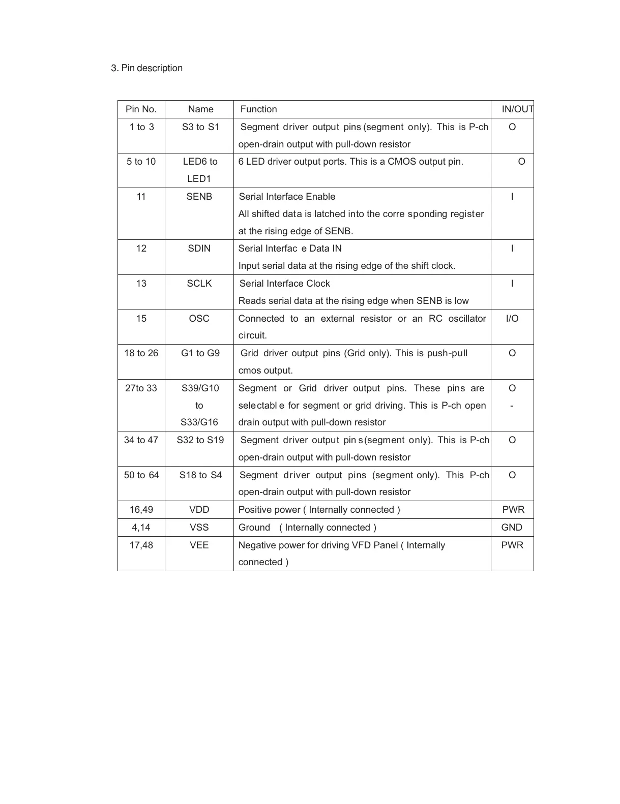
Pin No. Name Function IN/OUT
1 to 3 S3 to S1 Segment driver output pins (segment only). This is P-ch
open-drain output with pull-down resistor
O
5 to 10 LED6 to
LED1
6 LED driver output ports. This is a CMOS output pin. O
11 SENB Serial Interface Enable
All shifted data is latched into the corre sponding regist er
at the rising edge of SENB.
I
12 SDIN Serial Interfac e Data IN
Input serial data at the rising edge of the shift clock.
I
13 SCLK Serial Interface Clock
Reads serial data at the rising edge when SENB is low
I
15 OSC Connected to an external resistor or an RC oscillator
circuit.
I/O
18 to 26 G1 to G9 Grid driver output pins (Grid only). This is push-pull
cmos output.
O
27to 33 S39/G10
to
S33/G16
Segment or Grid driver output pins. These pins are
selectabl e for segment or grid driving. This is P-ch open -
drain output with pull-down resistor
O
34 to 47 S32 to S19 Segment driver output pin s (segment only). This is P-ch
open-drain output with pull-down resistor
O
50 to 64 S18 to S4 Segment driver output pins (segment only). This P-ch
open-drain output with pull-down resistor
O
16,49 VDD Positive power ( Internally connected ) PWR
4,14 VSS Ground ( Internally connected ) GND
17,48 VEE Negative power for driving VFD Panel ( Internally
connected )
PWR
3. Pin description
 Loading...