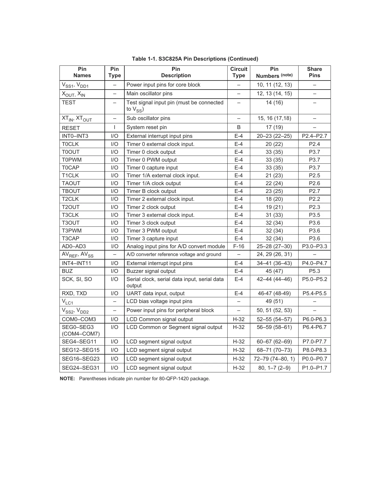
Table 1-1. S3C825A Pin Descriptions (Continued)
Pin
Names
Pin
Type
Pin
Description
Circuit
Type
Pin
Numbers
(note)
Share
Pins
V
SS1
, V
DD1
– Power input pins for core block – 10, 11 (12, 13) –
X
OUT
,
X
IN
– Main oscillator pins – 12, 13 (14, 15) –
TEST – Test signal input pin (must be connected
to V
SS
)
–14 (16) –
XT
IN
, XT
OUT
– Sub oscillator pins – 15, 16 (17,18) –
RESET
I System reset pin B 17 (19) –
INT0–INT3 I/O External interrupt input pins E-4 20–23 (22–25) P2.4–P2.7
T0CLK I/O Timer 0 external clock input. E-4 20 (22) P2.4
T0OUT I/O Timer 0 clock output E-4 33 (35) P3.7
T0PWM I/O Timer 0 PWM output E-4 33 (35) P3.7
T0CAP I/O Timer 0 capture input E-4 33 (35) P3.7
T1CLK I/O Timer 1/A external clock input. E-4 21 (23) P2.5
TAOUT I/O Timer 1/A clock output E-4 22 (24) P2.6
TBOUT I/O Timer B clock output E-4 23 (25) P2.7
T2CLK I/O Timer 2 external clock input. E-4 18 (20) P2.2
T2OUT I/O Timer 2 clock output E-4 19 (21) P2.3
T3CLK I/O Timer 3 external clock input. E-4 31 (33) P3.5
T3OUT I/O Timer 3 clock output E-4 32 (34) P3.6
T3PWM I/O Timer 3 PWM output E-4 32 (34) P3.6
T3CAP I/O Timer 3 capture input E-4 32 (34) P3.6
AD0–AD3 I/O Analog input pins for A/D convert module F-16 25–28 (27–30) P3.0–P3.3
AV
REF
, AV
SS
– A/D converter reference voltage and ground – 24, 29 (26, 31) –
INT4–INT11 I/O External interrupt input pins E-4 34–41 (36–43) P4.0–P4.7
BUZ I/O Buzzer signal output E-4 45 (47) P5.3
SCK, SI, SO I/O Serial clock, serial data input, serial data
output
E-4 42–44 (44–46) P5.0–P5.2
RXD, TXD I/O UART data input, output E-4 46-47 (48-49) P5.4-P5.5
V
LC1
– LCD bias voltage input pins – 49 (51) –
V
SS2
, V
DD2
– Power input pins for peripheral block – 50, 51 (52, 53) –
COM0–COM3 I/O LCD Common signal output H-32 52–55 (54–57) P6.0-P6.3
SEG0–SEG3
(COM4–COM7)
I/O LCD Common or Segment signal output H-32 56–59 (58–61) P6.4-P6.7
SEG4–SEG11 I/O LCD segment signal output H-32 60–67 (62–69) P7.0-P7.7
SEG12–SEG15 I/O LCD segment signal output H-32 68–71 (70–73) P8.0-P8.3
SEG16–SEG23 I/O LCD segment signal output H-32 72–79 (74–80, 1) P0.0–P0.7
SEG24–SEG31 I/O LCD segment signal output H-32 80, 1–7 (2–9) P1.0–P1.7
NOTE: Parentheses indicate pin number for 80-QFP-1420 package.
 Loading...