9
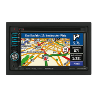
DNX4280BT/5180/5280BT/5380/5380M
/5380BT/5580BT/6040EX/6180/6480BT/6980
MICROCOMPUTER’S TERMINAL DESCRIPTION
●
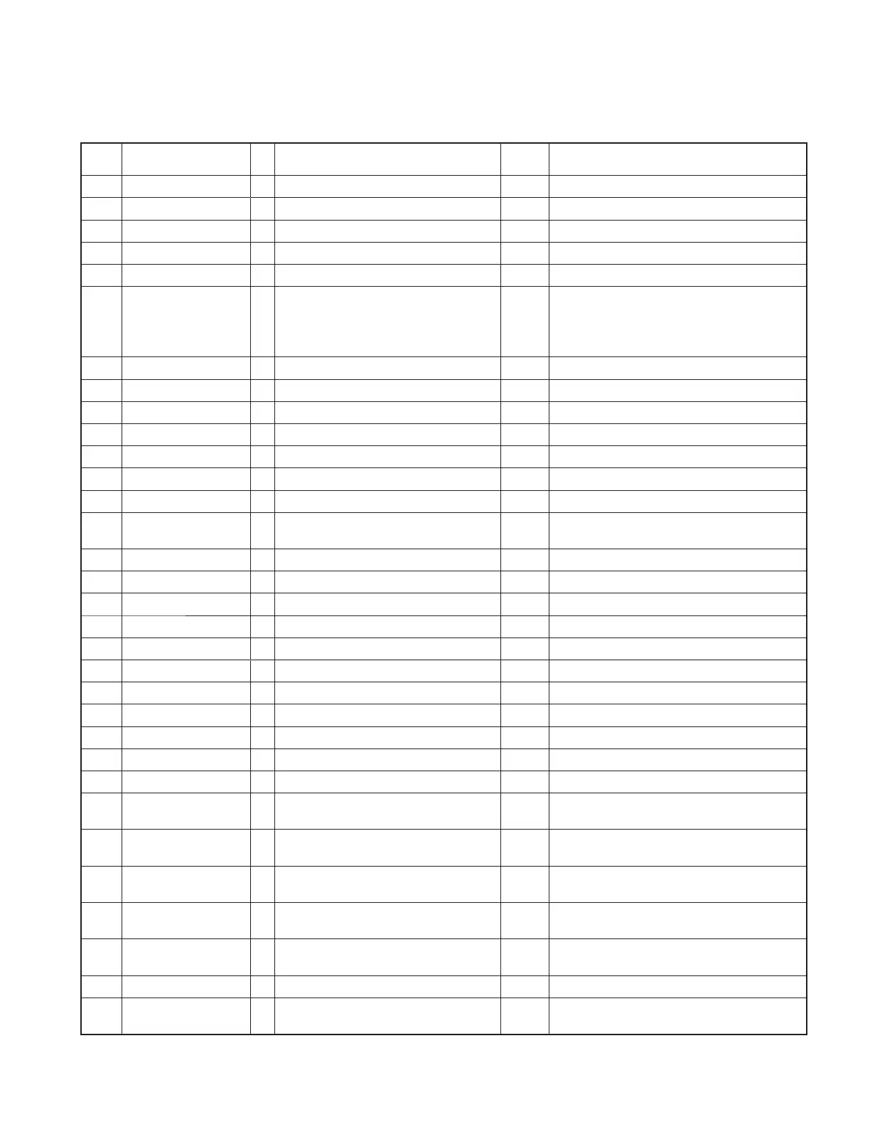
SYSTEM MICROCONTROLLER (X15 : IC205)
Pin No.
Pin Name I/O Application
Truth value
table
Processing / Operation / Description
1 VREF
2 AVCC
3 TV_SC_DATA I Data input from TV μ-com
4 TV_MC_DATA O Data output to TV μ-com
5 TV_BP_CLK O Communication clock with TV μ-com
6 SI (DSI) O SI (DSI) control
H: Off (at power-off), L: On (at power-on (in nor-
mal operation) Duty50%),
Intermittent operation (2S interval, L width
100ms): Blinking (at ACC off)
7 LV5680P O LV5680P control
8 R_DATA I “DATA” input from RDS decoder
9 WREMO I Remote controller input
10 R_QUAL I “QUAL” input from RDS decoder
11 TV_MC_REQ O Request to TV μ-com
12 TV_SC_CON O Request to start-up TV μ-com
13 BYTE I External data bus width switching input In single chip mode: Connected to VSS
14 CNVSS I Processor mode switching terminal
In microprocessor mode: Connected to VCC1
In single chip mode: Connected to VSS
15 XCIN Sub-clock oscillation circuit input 32.768kHz (crystal oscillator)
16 XCOUT Sub-clock oscillation circuit output 32.768kHz (crystal oscillator)
17 RESET Reset input L: Reset, H: Reset clear
18 XOUT Main clock oscillation circuit output 12MHz (crystal oscillator)
19 VSS
20 XIN Main clock oscillation circuit input 12MHz (crystal oscillator)
21 VCC1
22 NMI
23 TV_SC_REQ I Request from TV μ-com
24 R_CLK I Clock input from RDS decoder
25 PANEL_DET I PANEL detach / attach detection H: Detach, L: Attach
26 R_AFS_H I/O
Time constant switching when F/E noise
is detected
27
EVOL_SCL/ASEL_SCL/
E2PROM_SCL/DSP_SCL
O Communication clock with E-VOL
27
EVOL_SCL/ASEL_SCL/
E2PROM_SCL/DSP_SCL
O Communication clock with AV selector
27
EVOL_SCL/ASEL_SCL/
E2PROM_SCL/DSP_SCL
O
Communication clock with EEP
(External memory)
27
EVOL_SCL/ASEL_SCL/
E2PROM_SCL/DSP_SCL
O Communication clock with simplifi ed DSP
28
TUN_IFC
I F/E IFC input H: Station found, L: Station not found
29
EVOL_SDA/ASEL_SDA/
E2PROM_SDA/DSP_SDA
I/O Communication data with E-VOL
 Loading...