NXR-700H
16
TX Mod
19.2MHz
PLL circuit
IC307
5V #2
5V #1
19.2MHz
Q211
CF201
5V #1
4.5MHz
Q212
5V #1
Q213
5V #1
TX main
PLL circuit
4.5MHz
IC202
DDS IC
ATT ATT
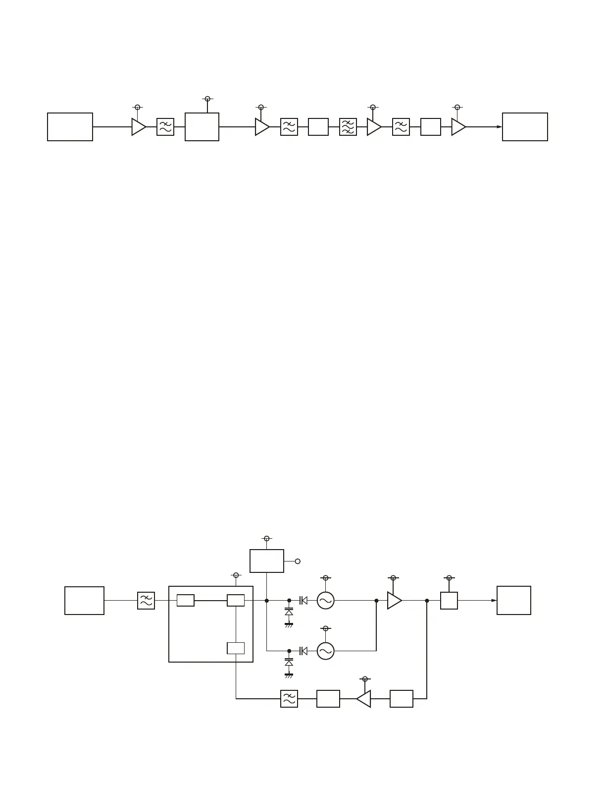
Fig. 4 Transmitter DDS circuit /
图 4 发射机 DDS 电路
2-5. Transmitter main PLL circuit
The transmitter main PLL circuit consists of the VCO
(Q102 and Q103), PLL IC (IC101) and divide-by-2 circuit
(IC811) and produces the transmitter frequency signal.
The VCO Q102 produces transmitter frequencies from
146.000MHz to 159.995MHz. (The transmitter frequency of
the VCO is from 292.000MHz to 319.990MHz.)
The VCO Q103 produces transmitter frequencies from
160.000MHz to 174.000MHz. (The transmitter frequency of
the VCO is from 320.000MHz to 348.000MHz.)
The signal produced by the VCO (Q102 or Q103) is fed to
the buffer amplifi er and is amplifi ed by Q106. The higher
harmonic wave is attenuated by LPF and returns to the PLL
IC (IC101).
IC101 divides the VCO oscillating frequency signal and
transmitter PLL reference signal (4.5MHz), and compares
the phase with the 100kHz comparison frequency.
The phase difference signal produced by the comparing
phase is converted to a DC voltage by a lag-lead type loop
fi lter.
The DC signal is applied to varicaps D101, D102, D107,
and D108 to lock the VCO oscillator frequency with the de-
sired oscillator frequency.
At the same time, the DC signal passes through the
IC102 operational amplifier for monitoring the transmitter
main PLL lock voltage.
The output from the VCO passes through the buffer am-
plifi er Q104. The divide-by-2 circuit (IC811) divides the fre-
quency and produces the transmitter frequency. The output
level of IC811 is about +6dBm (4mW).
Q106
TX DDS
circuit
1/R
1/N
PD
Fref.=4.5MHz
R=45
Fpd=100kHz
5V #2
Q104Q102
9V’ 9V’
3V
9V’
5V #2
292~
319.99MHz
292~
348MHz
IC102
OP-AMP
IC811
49
6
4.5MHz
IC101
PLL IC
CVT
Driver
circuit
146~
174MHz
D108
D107D101
Q103
9V’
320~
348MHz
D102
1/2
ATT
ATT
Fig. 5 Transmitter main PLL circuit /
图 5 发射机主 PLL 电路
CIRCUIT DESCRIPTION /
电路说明
2-5. 发射机主 PLL 电路
发射机主 PLL 电路由 VCO(Q102 和 Q103)、PLL IC(IC101)
和二分频电路 (IC811) 组成,产生发射机频率信号。
VC O Q102 产生 146.000MHz 至 159.995M Hz 的发射机频率。
(VCO 的发射机频率为 292.000MHz 至 319.990MHz。)
VC O Q103 产生 160.000MHz 至 174.000M Hz 的发射机频率。
(VCO 的发射机频率为 320.000MHz 至 348.000MHz。)
VCO(Q102 或 Q103) 产生的信号被送到缓冲放大器,由 Q106
放大。较高的谐波由 LPF 衰减并返回 PLL IC(IC101)。
I C101 分 离 V C O 振荡频率信号和发射机PLL 基准信号
(4.5MHz),与 100kHz 对比频率的相位进行比较。
通过相位对比产生的相位差信号由一个滞后超前式环路滤
波器转换为 DC 电压。
DC 信号施加于变容二极管 D101、D102、D107 和 D108,以
所需的振荡器频率锁定 VCO 振荡器频率。
与此同时,D C 信号通过用于监测发射机主 PL L 锁定电压的
IC102 运算放大器。
VC O 的输出通过缓冲放大器 Q104。二分频电路 ( I C811) 分
频并产生发射机频率。IC811 的输出电平约为 +6dBm(4mW)。

 Loading...