NXR-710
9
1. Outline
The NXR-710 is a VHF repeater operating in the 136~
174MHz frequency range.
2. TX-RX unit
TX-RX unit (X57-7940-10) consists of the following cir-
cuit.
(1) Internal/external reference circuit
(2) Transmitter reference 16.8MHz PLL circuit
(3) Transmitter main PLL circuit
(4) Modulation level adjustment circuit
(5) Front-end circuit
(6) 1st-Mixer circuit
(7) IF circuit
(8) Receiver PLL circuits
(9) AVR circuits
(10) Other circuits
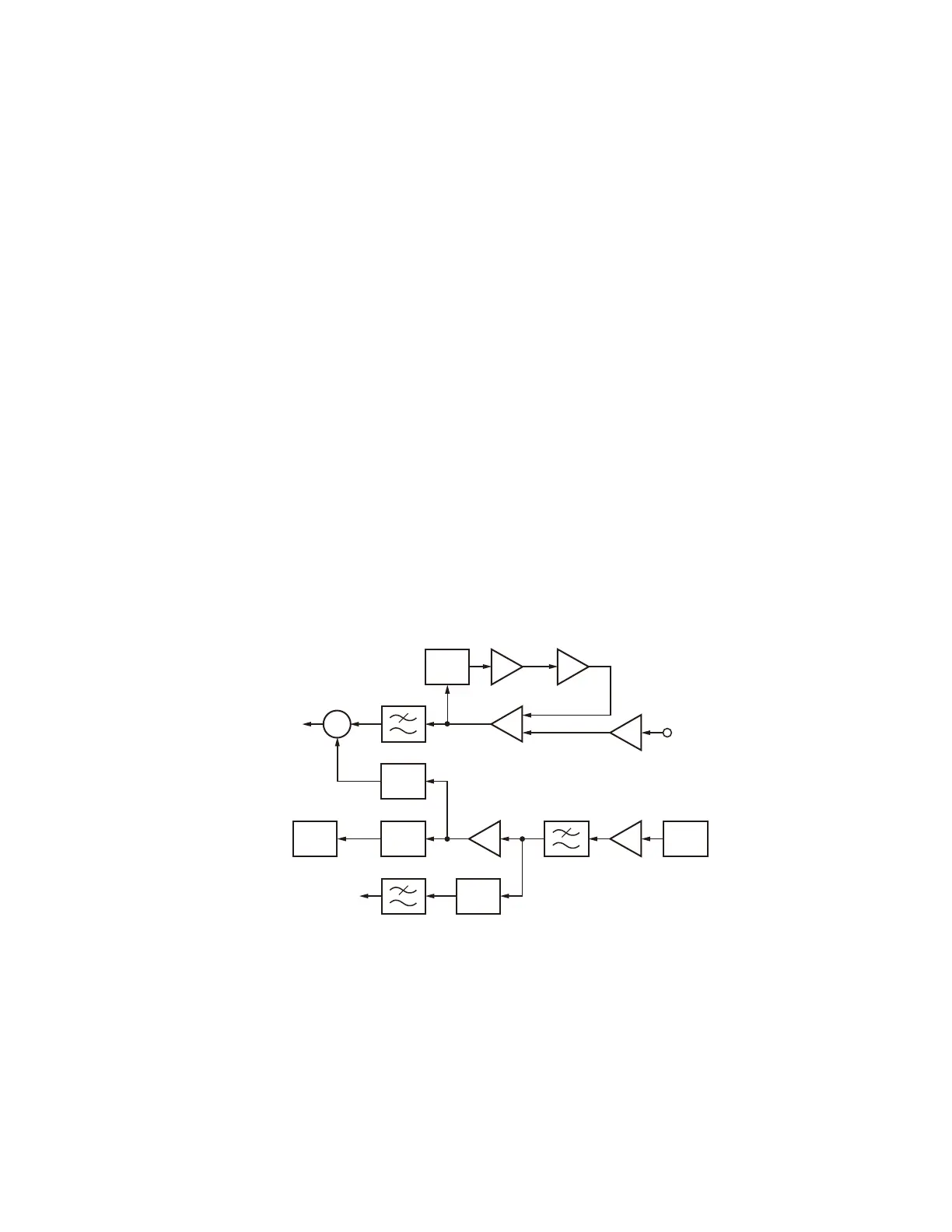
2-1. Internal/External reference circuit
The internal reference circuit consists of X500, Q502,
Q504 and D505. The output of 19.2MHz VCTCXO (X500) is
fed to buffer amplifi er Q502. The higher harmonic wave is
attenuated by the LPF. This reference signal is fed to IF IC
(IC304) as the 2nd Local signal through the Tripler.
The internal reference signal is amplified by Q504 to
achieve the needed level for PLL ICs. That signal is divided
by a Wilkinson divider. The divided signal is fed to the PLL
IC for the receiver. Another signal is fed to the transmitter
reference 16.8MHz PLL IC through PIN diode switch (D505)
which switches the Internal or external reference.
The external reference circuit consists of CN500, Q501,
Q503, IC500, IC501, D503 and D504. The external refer-
ence signal (10MHz/0dBm) input from CN500 is fed to buf-
fer amplifi er Q501 and is amplifi ed by Q503. Q503 is a dual
gate MOS-FET. The output of amplifi er (Q503) is detected
by D503 and that DC voltage is amplified by IC500 (B/2).
The amplifi ed DC voltage is compared to the reference volt-
age by IC500 (A/2). The difference of voltages is amplifi ed
by IC500 (A/2) and is fed to the gate-2 terminal of Q503. The
voltage of the Q503 gate-2 terminal is controlled automati-
cally to constantly maintain the power output of amplifier
(Q503). The output of amplifi er (Q503) is fed to the transmit-
ter reference 16.8MHz PLL IC through the PIN diode switch
(D504) which switches the Internal or External reference.
The PIN diode switches (D504, D505) are controlled by
the I/O expander IC (IC805 Pin15). The I/O expander IC is
controlled by the MCU which is in the Control unit (X53-449).
If internal reference is selected by FPU, the I/O expander IC
outputs an “H” status. This signal sets power switch Q506
to ON. Then D505 is activated.
If external reference is selected, the I/O expander IC out-
puts an “L” status. This signal sets power switch Q500 to
ON. Then D504 is activated.
CIRCUIT DESCRIPTION
10MHz or
19.2MHz
Detector
RX VCO
/PLL
1dB
ATT
1dB
ATT
X58-5070-10
2nd Lo
REF
AMP
Q504
AMP
Q502
AGC AMP
Q503
Buffer
Q501
SW
X3
Q202LPF
LPF
CN500
LPF
D503
AMP
IC500(B/2)
AMP
IC500(A/2)
X500
OSC
19.2MHz
D504,D505
EXT_IN
10MHz
Fig. 1 Internal/external reference circuit
2-2. Transmitter reference 16.8MHz PLL circuit
The transmitter reference 16.8MHz PLL circuit produces
the reference frequency signal for the Transmitter Main PLL
circuit and modulates the low-frequency components.
The circuit consists of IC600, IC601, IC602, IC603,
IC604, Q601, Q602, Q603, and X600.
The VCXO (X600) signal enters the buffer amplifi er Q603
and is amplifi ed by Q602. The higher harmonic wave is at-
tenuated by the LPF and returns to IC602. Its phase is com-
pared with that of the reference frequency 5kHz.
The phase difference signal produced by the comparing
phase is converted to a DC voltage by a lag-lead type loop
fi lter. This DC voltage is input to the IC604 invert amplifi er
and is synthesized with the modulating signal. This DC volt-
age is input to the X600 control voltage terminal for control-
ling the VCXO oscillating frequency 16.8MHz.
The 16.8MHz oscillating signal is fed to the Q603 buffer
amplifi er. The output signal of the buffer amplifi er is used as
the reference frequency signal of the transmitter main PLL
circuit.
 Loading...