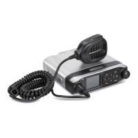
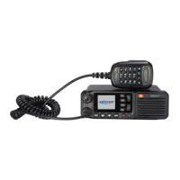
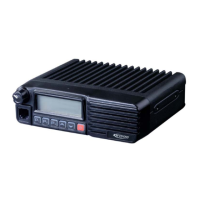
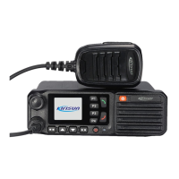
DM588 Service Manual
The radio is powered by a car battery, and the baseband circuit and the RF circuit are powered
independently. A protection unit at the front end of the power supply detects overvoltage and
overcurrent to ensure safety.
To the baseband circuit, the MP2359 DC-DC convertor outputs a voltage of 4.2V to power the master
chip LT1901 and the PMU in the Bluetooth chip, and the PMU of the LT1901 outputs 3M, AVDD_2V8,
USB3.3V, D1V8 and D1V2A to power other parts.
The radio is powered on or off through control over the inhibit pin of a DC/DC convertor.
For startup, the On/Off key is held down, the POWER_KEY is at a low logic level, the DC/DC circuit is
put through via a logic conversion circuit, the system is powered on and initialized, and the
POWER_HOLD is set to a high level to keep the DC/DC convertor enabled until startup is finished.
For poweroff, the system detects that the On/Off key is held down, executes the poweroff process,
and finally sets the POWER_HOLD to a high level to cut off the DC/DC circuit.
4.6.Others
Bluetooth and GPS are provided as required in orders.
4.7.Port Description of Master Chip LT1901
A11 GPIO_D46 5SC
Power switch of phase-locked loop (on at
Receiving power switch (on at high level)
E13 GPIO_D48 5TC Transmitting power switch (on at high level)
E12 GPIO_D50 TXENABLE
Enable transmitting power amplification
Hold power for soft startup
Enable GPS receiving (valid at high level)
Output GPS/4G module data
J18 TXD1 TXD1 Input GPS/4G module data
T18 GPIO_D109 GPS/4G_SELECT Select GPS/4G module
J14 RXD0 RXD0 Output BT chip data
J15 TXD0 TXD0 Input BT chip data
F9 GPIO_D54 TXRX Select TX/RX VCO
B10 GPIO_D56 SPI_DATA SPI data (phase-locked loop, IF chip, DAC)
B11 GPIO_D57 SPI_CLK
SPI clock (phase-
DAC)
C11 GPIO_D55 72310_LD Phase-locked loop lock detection
A10 GPIO_D58 SPI_72310_CS Chip select of phase-locked loop
Power saving mode of IF chip
T19 GPIO_D14 PTT PTT key input
F10 GPIO_D0 HOCK Hand microphone hook
E10 GPIO_D3 CM 1-wire bus / external hand microphone key
7