3NC/3NB/3NK
2-3-8
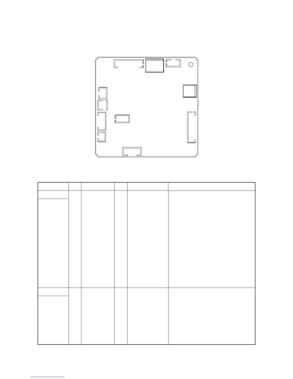
2-3-3 Punch unit PWB
Figure 2-3-3 Punch unit PWB silk-screen diagram
Connector Pin Signal I/O Voltage Description
YC1 1 PH_SDI I 0/3.3V DC(pulse) Serial communication data signal input
Connected to
the machine
2 PH_SDO O 0/3.3V DC(pulse) Serial communication data signal output
3 PH_CLK I 0/3.3V DC(pulse) Serial communication clock signal
4 PH_SEL I 0/3.3V DC Select signal from the machine
5 PH_RDY O 0/3.3V DC Ready signal to the machine
6 PHMOT_REQ I 0/3.3V DC PUM: On/Off
7 PHPES_REQ O 0/3.3V DC PUPES: On/Off
8 GND - - Ground
9 GND - - Ground
10 3.3V I 3.3V DC 3.3 V DC power input from machine
11 3.3V I 3.3V DC 3.3 V DC power input from machine
12 5.0V I 5V DC 3.3 V DC power input from machine
YC2
1 GND - - Ground
Connected to
the machine
2 24V2 I 24V DC 24 V DC power input from machine
YC2
YC9
YC8
YC7
YC6
YC4
YC5
YC3
YC10
YC1
YC11
1
1
1
1
1
2
16
12
13
1
1
5
2
3
1
4
11
12
4