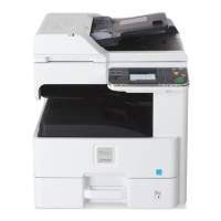
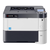
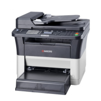
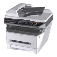
2K3/2L3
2-3-4
YC105 26 OVSYNCMON O 0/3.3 V DC Sub-scanning monitor signal
Connected to
engine PWB
27 PAGEST I 0/3.3 V DC Sub-scanning standard signal
28 EME_CLK O 0/3.3 V DC(pulse) Clock signal
29 EME_SO O 0/3.3 V DC(pulse) Serial communication data signal output
30 EME_SI I 0/3.3 V DC(pulse) Serial communication data signal intput
31 EME_BSY I 0/3.3 V DC Busy signal
32 EME_DIR I 0/3.3 V DC Communication direction change signal
33 EME_IRN I 0/3.3 V DC Interrupt signal
34 5V4IL - DC5 V 5 V DC power input from EPWB
35 BDN O 0/3.3 V DC(pulse) Horizontal synchronizing signal
36 VCONT I Analog Leser control signal
37 OUTPEN I 0/3.3 V DC Laser output permission signal
38 N.C. - - Not used
YC106 1 GND - - Ground
Connected to
relay PWB
2 RLYREM O 0/5 V DC relay drive signal
3 5V0 I 5 V DC 5 V DC power input from RYPWB
YC107 1 VBUS O 5 V DC 5 V DC power output
Connected to
USB-HOST
2 DATA- I/O LVDS USB data signal
3 DATA+ I/O LVDS USB data signal
4 ID - - Not used
5 GND - - Ground
YC112 1 +24V4 O 24 V DC 24 V DC power output to LEDPWB
Connected to
exposure
lamp (LED
PWB)
2 +24V4 O 24 V DC 24 V DC power output to LEDPWB
3 POW O 0/3.3 V DC LED driver: On/Off
4 PWM O 0/3.3 V DC PWM signal
5 PGND - - Ground
6 SGND - - Ground
7 VSET O Analog Analog voltage
8 SCL O 0/3.3 V DC(pulse) Clock signal
9 SDA I/O 0/3.3 V DC(pulse) Data signal
10 FAIL I 0/3.3 V DC Error signal
11 5V4 O 5 V DC 5 V DC power output to LEDPWB
Connector Pin Signal I/O Voltage Description
 Loading...
