MPX G2 Service Manual
6-8
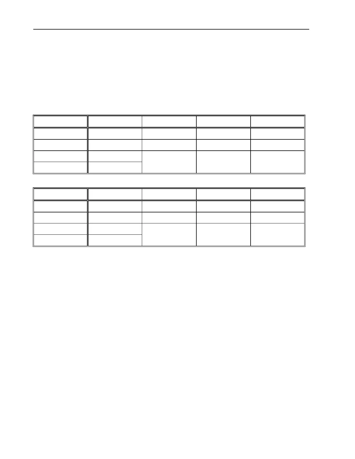
Memory Map:
The EPROM is divided into 8 32K banks. The Z80 selects the bank by writing to the I register, whose
contents are placed on the high address bus during refresh. The three extended address lines (labeled
P15-P17 on the schematic) are mapped into the I register as follows:
D7 D6 D5 D4 D3 D2 D1 D0
P17 P16 P15
ADDRESS BANK 0 BANK 1 BANK 2 BANK 3
0x0000 COMMON ROM COMMON ROM COMMON ROM COMMON ROM
0x4000 see below see below see below see below
0x8000 COMMON ROM ROM BANK 1 ROM BANK 2 ROM BANK 3
0xC000 ROM BANK 0
ADDRESS BANK 4 BANK 5 BANK 6 BANK 7
0x0000 COMMON ROM COMMON ROM COMMON ROM COMMON ROM
0x4000 see below see below see below see below
0x8000 ROM BANK 4 ROM BANK 5 ROM BANK 6 ROM BANK 7
0xC000 ROM BANK 4
When A15 is low, the Z80 addresses either the common ROM, or the memory-mapped peripherals defined
below. When A15 is high, the Z80 addresses the ROM bank selected by P15-P17.
The 2186 can't drive A14 or A15. When it takes over the bus, A15 is pulled low and A14 is pulled high,
allowing the 2186 to access memory-mapped peripherals in the "0x4000" block.
The 16K block between 0x4000 and 0x8000 contains the SRAM and memory-mapped peripherals. We
have to shoehorn a 32K SRAM into this area, so once again we use the same bank-switching technique as
with the EPROM. The Z80 sets bit 4 of the I register, called RAM_A14, to determine which bank it will
access. When the 2186 owns the bus, RAM_A14 is gated low.