I/O pin description
LGE Internal Use Only
Copyright © 2008 LG Electronics. Inc. All right reserved.
Only for training and service purposes
3. TECHNICAL BRIEF
- 67 -
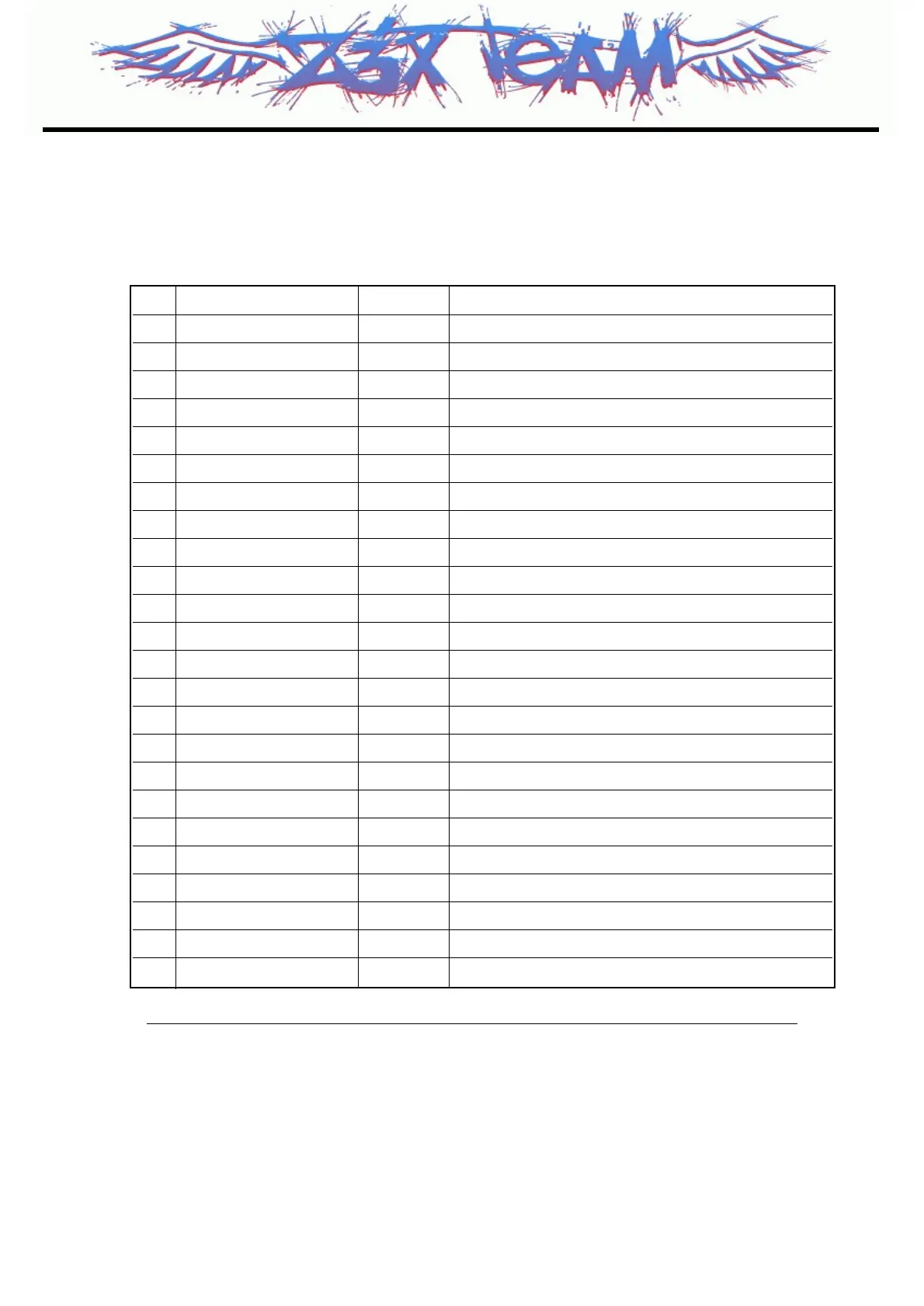
No Pin Name I/O Description
1 AGND G Analog GND
2D7ODigital Video data [7]
3D6ODigital Video data [6]
4D5ODigital Video data [5]
5D4ODigital Video data [4]
6D3ODigital Video data [3]
7D2ODigital Video data [2]
8D1ODigital Video data [1]
9D0ODigital Video data [0]
10 PCLK O Clock for output data
11 RESETB I RESET (Active Low)
12 STDBYB I Stand BY (Active Low)
13 DGND G GND
14 DVDD-CORE I 1.5V, Core Digital Power
15 IOVDD I 1.8V or 2.8V, I/O Digital Power
16 AVDD I 2.8V, Analog Power
17 DGND G Digital GND
18 MCLK I Master input clock
19 HSYNC O Horizontal Sync Signal
20 VSSYNC O Vertical Sync Signal
21 DGND G Digital GND
22 SDA I/O I
2
C Data
23 SCK I/O I
2
C Clock
24 AGND I Analog GND
[Table 3.12] Interface between MEGA Camera Module and MAIN PCB (in camera module)
 Loading...