LGE Internal Use Only
Copyright © 2008 LG Electronics. Inc. All right reserved.
Only for training and service purposes
3. TECHNICAL BRIEF
- 27 -
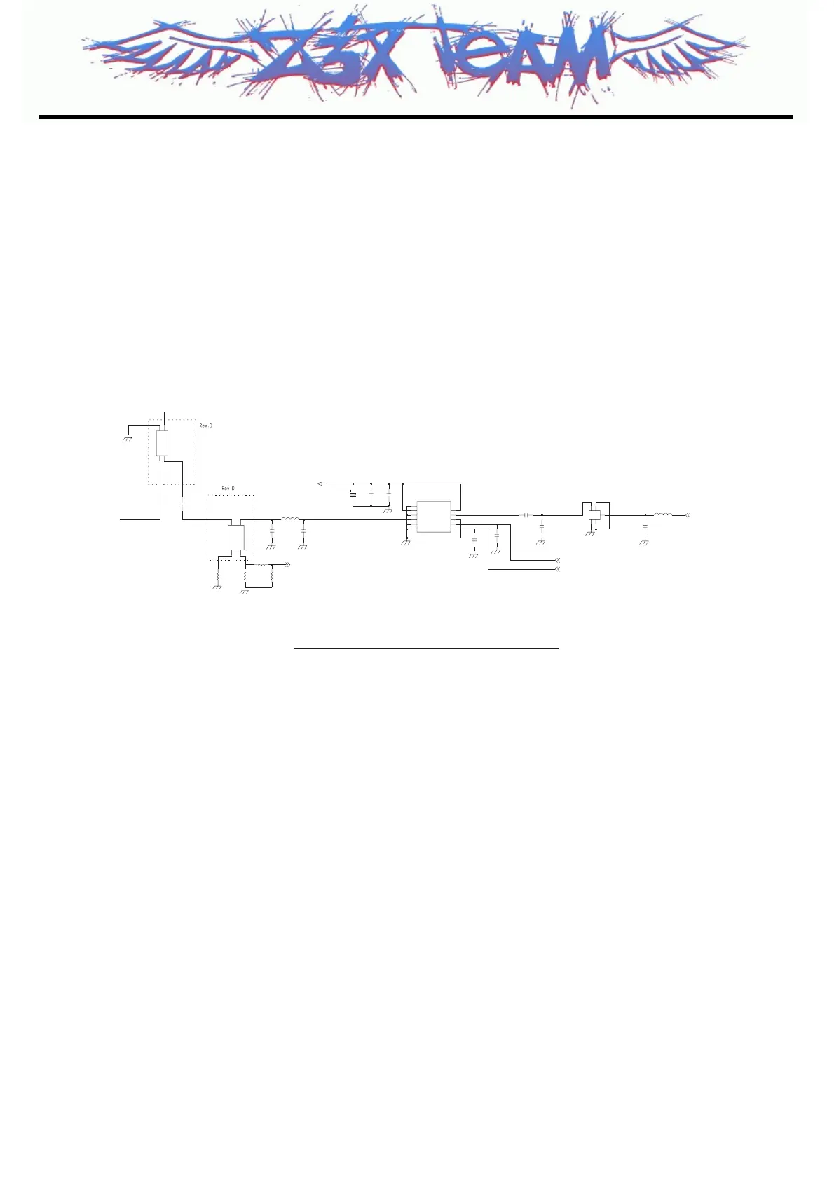
3.5 Off-chip RF Components
3.5.1 UMTS PAM (U105: ACPM-7381)
The UMTS PA output power is monitored by power detector circuits (U101 : RTR6275) .
This detector voltage can be used for transmitter calibration and monitor to meet RF system
specification.
3.5.2 VCTCXO (X101 : TG-5010LH(19.2M)-75A)
The Voltage Controlled Temperature Compensated Crystal Oscillator (VCTCXO) provides the reference
frequency for all RFIC synthesizers as well as clock generation functions within the MSM6280 IC. The
oscillator frequency is controlled by the MSM6280 ICs. TRK_LO_ADJ pulse density modulated signal in
the same manner as the transmit gain control TX_AGC_ADJ. A two-pole RC lowpass filter is
recommended on this control line.
The PM6650 IC controls the handset power-up sequence, including a special VCTCXO warm-up
interval before other circuits are turned on. This warm-up interval (as well as other TCXO controller
functions) is enabled by the MSM TCXO_EN line. The PM6650 IC VREG_TCXO regulated output
voltage is used to power the VCTCXO and is enabled before most other regulated outputs.
Any GSM mode power control circuits within the MSM6280 IC require a reference voltage for proper
operation and sufficient accuracy. Connecting the PM6650 IC REF_OUT directly to the MSM6275 IC
GSM_PA_PWR_CTL_REF provides this reference. This sensitive analog signal needs a 0.1 µF low
frequency filter near to MSM side, and isolate from digital logic and clock traces with ground on both
sides, plus ground above and below if routed on internal layers.
 Loading...