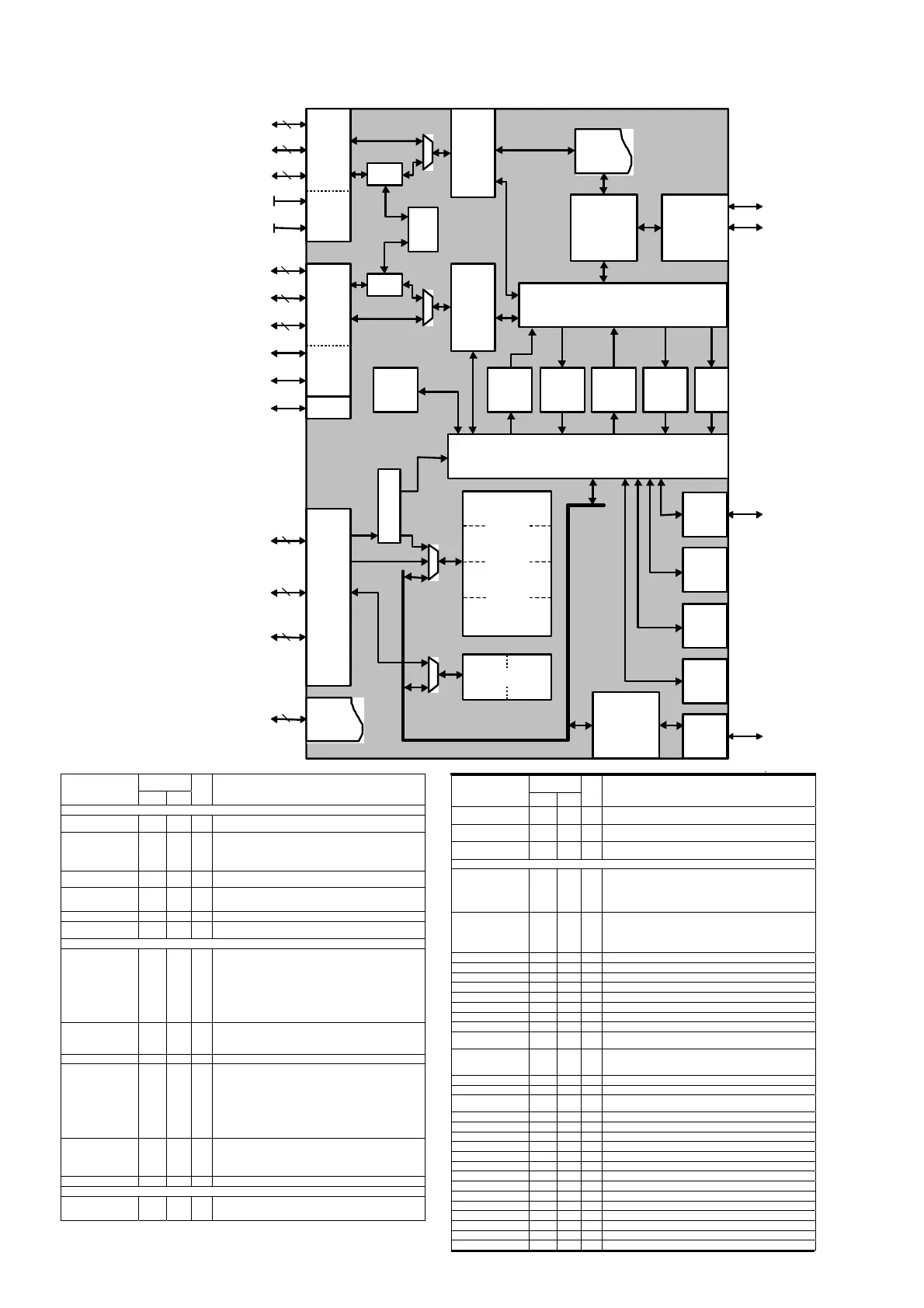
[PI01] QI01 : TSB43CA42PGF
MPEG2 DVB
MPEG2 DSS
DIGITAL VIDEO (DV)
PCM-AUDIO
IEC60958 (S/PDIF)
OR
OR
OR
OR
HSDI 0
ISO
PORT
8
8
8
ISO
HSDI 0
FIFO
4KB
MPEG2 DVB
MPEG2 DSS
DIGITAL VIDEO (DV)
SUPER AUDIO CD
IEC60958 (S/PDIF)
PCM-AUDIO
OR
OR
OR
OR
OR
8
8
8
ISO
HSDI 1
FIFO
4KB
M6
CIPHER
H / W
AKE
L
E
B
256KB RAM
PROGRAM
MEMORY
AND
COMM
MEMORY
SHARED RAM
1KB 1KB
CONFIGURATION REGISTERS (CFRs)
JTAG
PORT
TIMER 0
WDOG /
TIMER 2
TIMER 1
1394a-2000
LINK LAYER
CORE
PACKETIZER
ARM7TDMI
RISC
CORE
UART
EXT.
MCU
I/F
16
10
20
DATA
ADDRESS
CONTROL
1394a-2000
S400
2-PORT
PHY CORE
CFRs
1394
BUS
ARM
DEBUGGER
MONITOR
CFRs
11
GP I/O
AUDIO
RX
SYT PLL
ASYNC
TX 0 FIFO
2KB
ASYNC
TX 1 FIFO
2KB
ASYNC
RX 0 FIFO
2KB
ASYNC
RX 1 FIFO
2KB
BCAST
RX
FIFO
512 B
M6
CIPHER
HSDI 1
ISO
PORT
Terminal
Number
Terminal Name
BGA QFP
I/O Description
Miscellanous Pins
DISABLE_IFn T8 64 I
Interface disable. When asserted, the interfaces are put into a high-Z
state. Interfaces include: ex-CPU, HSDI, GPIO, and WTCH_DG_TMRn.
HPS P8 62 I
Host power status. This indicates the power status of the external system
to iceLynx-Micro. A rising edge indicates the system CPU has been turned
ON. (The internal ARM must wake up.) A falling edge indicates the system
CPU has been turned OFF. (The internal ARM decides if power down is
necessary.)
LOW_PWR_RDY R8 63 O
Output to system to indicate iceLynx-Micro is ready to go into a low power
state. The ARM and WTCH_DG_TMRn control this pin.
WTCH_DG_TMRn U16 88 O
Watch dog timer (for the ARM). iceLynx-Micro hardware asserts this pin
whenever ARM software has not updated the Timer2 register within the
allowed time period.
RESET_ARMn U7 60 I ARM reset. This signal resets the internal ARM processor.
RESETn T7 59 I
Device reset. This signal resets all logic. This includes the PHY, link core,
memory, the ARM, and random logic.
Power and Ground Pins
VSS
A2,
B1,
B7,
C11,
C16,
G17,
J1,
L15,
P11,
T6
1, 21,
55,
76,
102,
117,
131,
146,
162,
176
Digital ground
AGND
J2, K4,
M3,
U2
24,
27,
35,
45,
Analog ground
PLL_GND R6 54 PLL ground
VDD
A7,
B3,
C17,
D3,
D11,
H2,
H15,
L14,
R11,
U6
4, 20,
56,
75,
101,
116,
130,
145,
161,
175
Digital power supply. Must be set to 3.3-V nominal.
AVDD
J3, K3,
L4,
P3, R4
23,
28,
32,
41,
48
Analog power supply. Must be set to 3.3-V nominal.
PLL_VDD R5 51 PLL power supply. Must be set to 3.3-V nominal.
Regulator Pins
REG_ENn U11 73 I
Internal regulator enable. The iceLynx-Micro core voltage is 1.8 V. Internal
regulators are used to regulate the 3.3-V VDD inputs to 1.8 V. This pin
enables the regulators.
p
Terminal
Number
Terminal Name
BGA QFP
I/O Description
REG_OUT0 T11 74 O
1.8-V regulator output. This pin must be connected to ground using a
0.1-PF capacitor.
REG_OUT1 H14 115 O
1.8-V regulator output. This pin must be connected to ground using a
0.1-PF capacitor.
REG_OUT2 C8 160 O
1.8-V regulator output. This pin must be connected to ground using a
0.1-PF capacitor.
External CPU Interface Pins
MCIF_ACKz N15 95 I/O
MCIF acknowledge pin. Default active low. iceLynx-Micro asserts this
signal if it has completed the MCIF request. This signal is driven when
chip select (CS) is asserted. This signal is used for the following modes:
68000 + wait I/O access
I/O Type-3 MPC850
MCIF_ADDR1 G14 120 I
MCIF address 1 pin. This data pin is the least significant bit of the MCIF
address bus.
MCIF_ADDR0 is internally grounded. Only 16-bit addressing is allowed.
MCIF_ADDR1 must be connected to the Address1 signal of the system
CPU.
MCIF_ADDR2 F17 121 I MCIF address 2 pin
MCIF_ADDR3 F16 122 I MCIF address 3 pin
MCIF_ADDR4 F15 123 I MCIF address 4 pin
MCIF_ADDR5 E17 124 I MCIF address 5 pin
MCIF_ADDR6 E16 125 I MCIF address 6 pin
MCIF_ADDR7 E15 126 I MCIF address 7 pin
MCIF_ADDR8 D17 127 I MCIF address 8 pin
MCIF_ADDR9 D16 128 I MCIF address 9 pin
MCIF_ADDR10 D15 129 I
MCIF address 10 pin. This data pin is the most significant bit of the MCIF
address bus.
MCIF_BUSCLKz M15 98 I
MCIF bus clock. This pin is only used for the MCIF synchronous mode. I/O
Type-3 MPC850 and the memory access.
This signal must be pulled high if not used.
MCIF_CS_IOz R16 90 I MCIF chip select for all I/O MCIF modes.
MCIF_CS_MEMz R17 91 I MCIF chip select for the memory MCIF mode.
MCIF_DATA0 M16 99 I/O
MCIF data 0 pin. This data pin is the least significant bit of the MCIF
data bus.
MCIF_DATA1 M17 100 I/O MCIF data 1 pin
MCIF_DATA2 L16 103 I/O MCIF data 2 pin
MCIF_DATA3 L17 104 I/O MCIF data 3 pin
MCIF_DATA4 K17 105 I/O MCIF data 4 pin
MCIF_DATA5 K14 106 I/O MCIF data 5 pin
MCIF_DATA6 K15 107 I/O MCIF data 6 pin
MCIF_DATA7 K16 108 I/O MCIF data 7 pin
MCIF_DATA8 J17 109 I/O MCIF data 8 pin
MCIF_DATA9 J14 110 I/O MCIF data 9 pin
MCIF_DATA10 J15 111 I/O MCIF data 10 pin
MCIF_DATA11 J16 112 I/O MCIF data 11 pin
MCIF_DATA12 H17 113 I/O MCIF data 12 pin
MCIF_DATA13 H16 114 I/O MCIF data 13 pin
MCIF_DATA14 G16 118 I/O MCIF data 14 pin
170