1. IC's
SEMICONDUCTORS
R5F5631FDDFB(DIGITAL_MCU : IC751)
Terminal Functions
Pin Pin Name Symbol I/O Pu/Pd STBY STOP
CEC
STBY
Function
1 AVSS0 AVSS - - - - Ground pin
2 P05/IRQ13 POWER_KEY I
M3VPu
I I I
Detect Power switch (Release from Wait Mode,Set to
interrupt)
3 VREFH VREFH - - - - Reference power supply pin
4 P03/IRQ11 RED_LED O L/H L H POWER/STANDBY LED control pin
5 VREFL VREL - - - - Ground pin
6 P02/IRQ10/AN020 DIRECT_LED O L L L DIRECT LED Control pin
7
P01/RXD6/IRQ9/
AN019
RXD_MI232O I
Pd
I I I
External data input port (for AMX/FW update via 232C)
:Connector is FFC
8
P00/TXD6/IRQ8/
AN018
TXD_MO232I O L L L
External data output port (for AMX/FW update via 232C)
:Connector is FFC
9 PF5/IRQ4
WHITE_
LED(X1400(NA)/
GREEN_
LED(X1400(AP/
CH)/S730)
O L L L POWER LED control pin
10 EMLE EMLE I
Pd
- - -
E20 Emulator control pin (On chip Emulator is used,this
pin should be High. Not used,it should be Low)
11 PJ5 VSEL_A I
SW3VPu
I I I Master volume (Rotary encoder) signal input pin
12 VSS VSS - - - - Ground pin
13 PJ3 VSEL_B I
SW3VPu
I I I Master volume (Rotary encoder) signal input pin
14 VCL VCL I - - - Smoothing capacitor connection pin
15 VBATT VBATT - - - - Power supply pin
16 MD/FINED MD I
M3VPu
I I I
Pins for setting the operating mode(select the Boot
Mode or User Boot Mode,Single Chip Mode)
17 XCIN XCIN I
Pd
- - - NC(Pull down)
18 XCOUT XCOUT I - - - NC(open)
19 RES# RESET I
M3VPu
- - - Reset signal input pin
20 XTAL/P37 XTAL I - - - Pins for a crystal resonator (Xin=10MHz × 10)
72
71
70
69
68
67
66
65
64
63
62
61
60
59
58
57
56
55
54
53
52
51
50
49
48
47
46
45
44
43
42
41
40
39
38
37
109
110
111
112
113
114
115
116
117
118
119
120
121
122
123
124
125
126
127
128
129
130
131
132
133
134
135
136
137
138
139
140
141
142
143
144
PE0
P64
P63
P62
P61
VSS
P60
VCC
PD7
PD6
PD5
PD4
PD2
PD1
PD0
P93
P92
P91
VSS
P90
VCC
P47
P46
P45
P44
P43
P42
P41
VREFL0
P40
VREFH0
P07
PE1
PD3
AVCC0
P74
PC2
P76
P77
PC3
PC4
P80
P81
P82
PC5
PC6
PC7
VCC
VSS
P50
P51
P52
P53
P54
P55
P56
VSS_USB
USB0_DP
USB0_DM
VCC_USB
P12
P13
P14
P15
P86
P16
P87
P20
P75
P83
P17
PE2
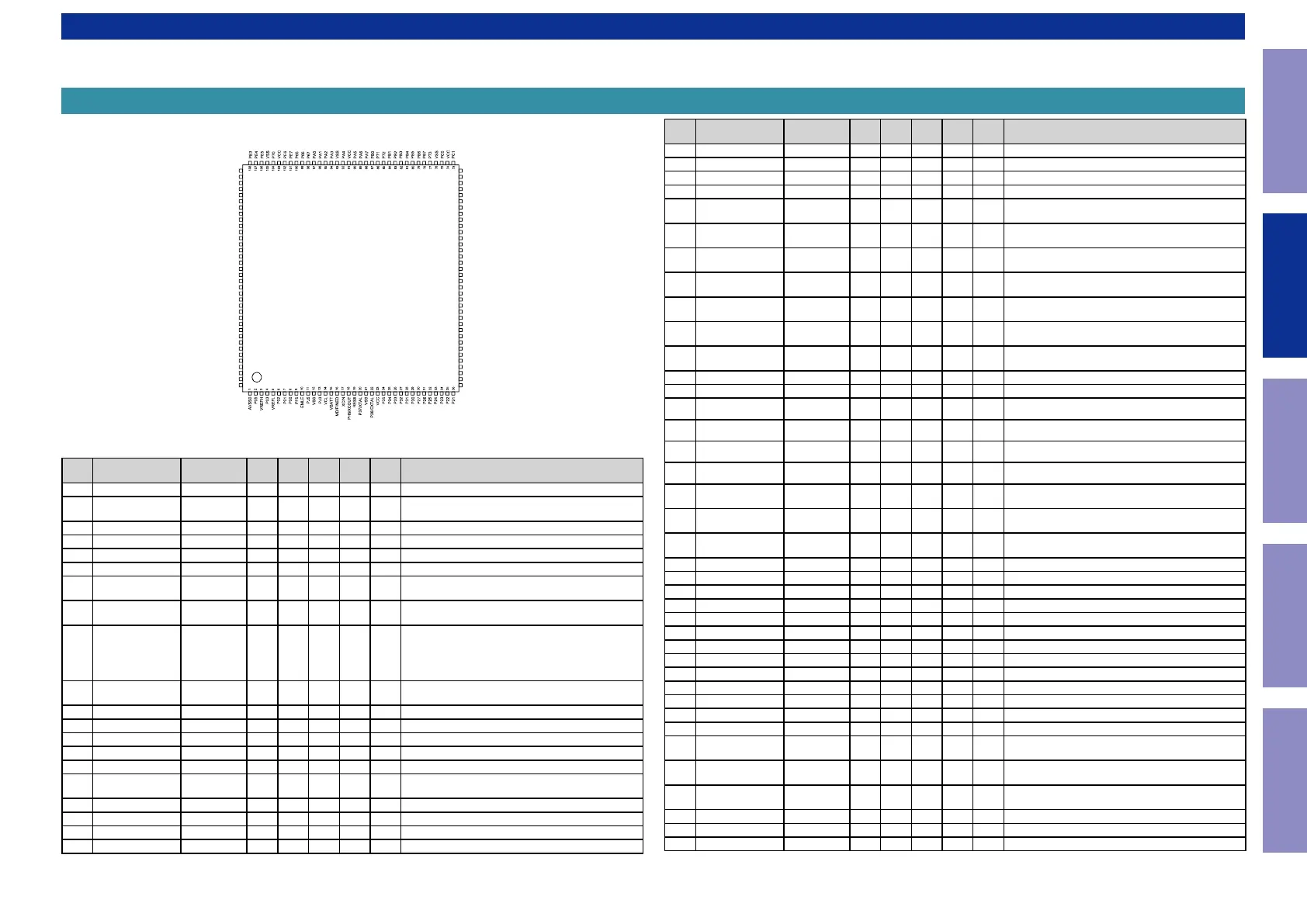
RX63N Group
RX631 Group
PLQP0144KA-A
(144-pin LQFP)
(Top view)
Note: This figure indicates the power supply pins and I/O port pins. For the pin configuration, see Table 1.8, List of
Pins and Pin Functions (144-Pin LQFP).
Pin Pin Name Symbol I/O Pu/Pd STBY STOP
CEC
STBY
Function
21 VSS VSS - - - - Ground pin
22 EXTAL/P36 EXTAL - - - - Pins for a crystal resonator (Xin=10MHz × 10)
23 VCC VCC - - - - Power supply pin.
24 P35(IN)/NMI DSP_FLAG0 I
Pd
L L L DSP(ADI) interrupt signal input pin
25 TRST#/P34/IRQ4
TRST#/
NC(NORMRAL)
I/I
Pd
I/I I/I I/I
E20 Emulator control pin/When normal operating
mode,set to input.
26
P33/TIOCD0/RXD6/
RXD0/IRQ3-DS
RC_IN I
M3VPu
I I I Remote input
27
P32/TXD6/TXD0/
IRQ2-DS
BDOWN I
M3VPu
I I I Detect power down
28 TMS/P31/IRQ1-DS
TMS/
NC(NORMRAL)
I/I
M3VPu
-/I -/I I
E20 Emulator control pin/When normal operating
mode,set to input.
29
TDI/P30/RXD1/
IRQ0-DS
TDI/RXD_MIT-
SUBISHI
I/O/I
M3VPu
-/-/I -/-/I I
E20 Emulator control pin/Mitsubishi writter control pin/
When normal operating mode,set to input.
30 TCK/FINEC/P27
TCK/
NC(NORMRAL)
I/I/I
M3VPu
-/-/I -/-/I I
E20 Emulator control pin//When normal operating
mode,set to input.
31 TDO/P26/TXD1
TDO/TXD_
MITSUBISHI
O/O/I
M3VPu
-/-/I -/-/I I
E20 Emulator control pin/Mitsubishi writter control pin/
When normal operating mode,set to input.
32 P25/RXD3 TU_IIC/RDSI O L L L TUNER control
33 P24 MVOL_MUTE O L L L Volume control pin (NJU72343)
34 P23/TXD3 E_RTS_MOEI O
Pd
(BCM58305
Internal Pd)
L L L Ethernet(LEGO) control pin
35 P22/SCK0 E_CTS_MIEO I
Pd
(BCM58305
Internal Pd)
I I I Ethernet(LEGO) control pin
36 P21/RXD0/IRQ9 E_RXD_MIEO I
Pd
(BCM58305
Internal Pd)
I L I Ethernet(LEGO) control pin
37 P20/TXD0/IRQ8 E_TXD_MOEI O
Pd
(BCM58305
Internal Pd)
L L L Ethernet(LEGO) control pin
38 P17/TXD3/IRQ7
NET_FACT_
RST
O(ODR)
Pu
(BCM58305
Internal Pu)
Z Z Z Ethernet(LEGO) control pin
39 P87
7623_ROM_
HOLD
O L L L Flash ROM for GUI control pin
40
P16/TXD1/RXD3/
IRQ6
NET5V_POW-
ER
O L L L Ethernet power supply (Net5V) control pin/
41 P86 NC O L L L
42 P15/RXD1/IRQ5 VEXP_STB O L L L Expander (MC14094) control pin
43 P14/IRQ4 VEXP_OE O L L L Expander (MC14094) control pin
44 P13/TXD2/IRQ3 VEXP_CLK O L L L Expander (MC14094) control pin
45 P12/RXD2/IRQ2 VEXP_DATA O L L L Expander (MC14094) control pin
46 VCC_USB VCC_USB - - - - Power supply pin
47 USB0_DM USB0_DM - - - - NC(open)
48 USB0_DP USB0_DP - - - - NC(open)
49 VSS_USB VSS_USB - - - - Ground pin
50 P56 TU_LA O L L L TUNER control pin
51 P55/IRQ10 TU_DA I_O
SW3VPu
L L L TUNER control
52 P54 TU_CK O
SW3VPu
L L L TUNER control
53 BCLK/P53 THERMAL_E I
SW3VPu
I L I PROTECTION Detection pin(Heat Sink)
54 P52/RXD2
ADV7623_
SPI_MI
I L L L HDMI transceiver w/ GUI(ADV7623) control pin (for GUI)
55 P51/SCK2
ADV7623_
SPI_CLK
O L L L HDMI transceiver w/ GUI(ADV7623) control pin (for GUI)
56 P50/TXD2
ADV7623_
SPI_MO
O L L L HDMI transceiver w/ GUI(ADV7623) control pin (for GUI)
57 VSS VSS - - - - Ground pin
58 P83 ADV7623_RST O
Pd
L L L HDMI transceiver w/ GUI(ADV7623) reset control pin
59 VCC VCC - - - - Power supply pin.
Only major semiconductors are shown, general semiconductors etc. are omitted to list.
The semiconductor which described a detailed drawing in a schematic diagram are omitted to list.
48
Caution in
servicing
Electrical Mechanical Repair Information Updating