Do you have a question about the Marantz NR1605/U1B and is the answer not in the manual?
Details how to use the search function in Acrobat Reader to find specific references.
Explains how to magnify diagrams using Ctrl+Space and mouse for better detail.
Details how to print specific magnified sections of the manual for reference.
Provides cautions regarding electrical shock, disassembly, parts handling, and wiring.
Instructs on wearing a grounding band to remove static electricity from the body.
Details power amplifier and analog section specifications.
Details standard video connectors and color component video connector specs.
Lists reception frequency range and sensitivity specifications.
Details wireless LAN standards, security, and frequency band.
Details Bluetooth communication system and supported profiles.
Lists power supply and power consumption specifications.
Details the procedure for initializing the unit after replacing components.
Details the disassembly of the front panel assembly.
Details the disassembly of the HDMI PCB.
Details the disassembly of the AV PCB.
Details the disassembly of the power transformer.
Details the disassembly of the SMPS PCB.
Lists buttons used to activate special modes for service.
Mode to display firmware versions and error information.
Mode to display protection occurrence history.
Initializes backup data including installer setup.
Allows power-on without activating protections.
Details the button sequence to start the panel/remote lock selection mode.
Lists the types of diagnostic modes available for service operations.
Details the button sequence to start these service modes.
Describes the purpose of the diagnostic mode for confirming problem paths.
Details the button sequence to start the diagnostic mode.
Explains what events are recorded and displayed in protection history.
Details the button sequence to start the protection history display mode.
Shows how to check protection history and example displays.
States what information this mode displays (operating time, power counts).
Details the button sequence to start the operation info mode.
Details the button sequence to start the tuner step mode.
Explains the purpose of the protection pass mode.
Details the button sequence to enter protection pass mode.
Explains when the reboot mode is used for the CX870/CY920.
Details the procedure for rebooting the CX870/CY920.
Lists the items that are initialized on the CX870/CY920.
Details the procedure to initialize the CX870/CY920.
Details items to prepare and procedures for connecting jigs to the HDMI PCB.
Explains software writing procedures after microprocessor or flash ROM replacement.
Explains how to update firmware using a USB memory.
Explains how to initiate the firmware update process.
Mode used when the unit cannot be recovered, forcing USB update.
Lists system requirements for network connection for firmware updates.
Explains how to check for and perform firmware updates via the internet.
Lists necessary preparations for adjusting idling current.
Provides step-by-step instructions for adjusting idling current.
Describes various Dolby sound modes like PLgx, Digital, TrueHD.
Describes various DTS sound modes like Neo:6, Surround, ES.
Addresses issues where the unit does not power on.
Troubleshooting steps for analog video output issues.
Flowchart for diagnosing no picture or sound from HDMI to HDMI connection.
Flowchart for checking audio output from various sources.
Flowchart for diagnosing network connection problems.
Flowcharts for diagnosing no picture or sound from USB devices.
Detailed schematic of the HDMI SW1 circuit.
Detailed schematic of the HDMI SW2 circuit.
Detailed schematic of the NET PHY circuit.
Detailed schematic of the Bluetooth module.
Detailed schematic of the CPU Level CHG circuit.
Detailed schematic of the DIGITAL CNT circuit.
Detailed schematic of the CPU.
Detailed schematic of the SUB CPU.
Detailed schematic of the FRONT HDMI circuit.
Detailed schematic of the DSP circuit.
Detailed schematic of the ADV8003 circuit.
Detailed schematic of the ADV8003 DDR memory interface.
Detailed schematic of the power supply circuits.
Detailed schematic of the HDMI transmitter circuit.
Detailed schematic of the DIR A.PLD circuit.
Detailed schematic of the V.PLD circuit.
Detailed schematic of the MAIN DAC circuit.
Detailed schematic of the ADV7850 circuit.
Detailed schematic of the CX870 JUNCTION circuit.
Detailed schematic of the AV section (part 1 of 3).
Detailed schematic of the AV section (part 2 of 3).
Detailed schematic of the AV section (part 3 of 3).
Detailed schematic of the 7-channel amplifier (part 1 of 2).
Detailed schematic of the 7-channel amplifier (part 2 of 2).
Detailed schematic of the speaker control circuit.
Detailed schematic of the side connector interface.
Detailed schematic of the front PCB.
Detailed schematic of the SMPS circuit.
Detailed schematic of the regulator control circuit.
Detailed schematic of the front connector interface.
Details pin functions for R5F56108VNFP (HDMI : U1018).
Shows the block diagram for the AD8195ACPZ.
Lists pin functions for the PCM9211 IC.
Shows the block diagram for PCM9211.
Shows the block diagram for PCM9211.
Details terminal functions for the ADSP21487KSWZ3B IC.
Shows the block diagram for W9864G6JH-6.
Details pin functions for the PCM1690 IC.
Shows the functional block diagram for PCM1690.
Shows the block diagram for PCM510x.
Details pin descriptions for R2A15218FP.
Shows the pin connection details for the FL display.
Details pin functions for R5F56108VNFP (HDMI : U1018).
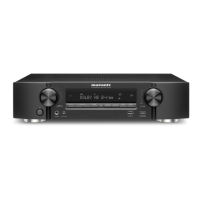
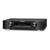
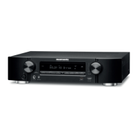
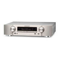
| Brand | Marantz |
|---|---|
| Model | NR1605/U1B |
| Category | Stereo Receiver |
| Language | English |