


M
Michael WyattSep 10, 2025
How to fix no audio output with HDMI connection on Marantz Stereo Receiver?
- OobakerSep 10, 2025
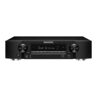
If you're experiencing no audio output with an HDMI connection on your Marantz Stereo Receiver, check the connection of the HDMI connectors. When outputting HDMI audio from the speakers, set “HDMI Audio Out” on the menu to “Amp.” When outputting HDMI audio from a TV, set “HDMI Audio Out” on the menu to “TV.”