1-37 1-38
Control
and
JTAG
Interface
Memory
Serial
Interface
DATA (D0)
Serial Mode
Data
Address
CLK CE
TCK
TMS
TDI
TDO
OE/RESET
CEO
Data
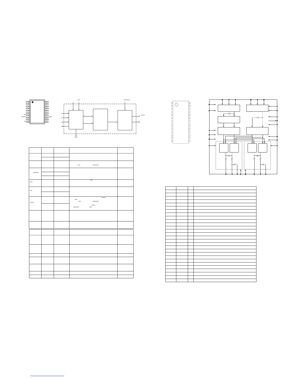
ds123_01_30603
CF
Pin Name
Boundary
Scan Order
Boundary
Scan Function Pin Description
20-pin TSSOP
(VO20/VOG20)
D0
4 Data Out
D0 is the DATA output pin to provide data for configuring an
FPGA in serial mode. The D0 output is set to a
high-impedance state during ISPEN (when not clamped).
1
3 Output Enable
CLK
0Data In
Configuration Clock Input. Each rising edge on the CLK input
increments the internal address counter if the CLK input is
selected, CE is Low, and OE/RESET is High.
3
OE/RESET
20 Data In
Output Enable/Reset (Open-Drain I/O). When Low, this input
holds the address counter reset and the DATA output is in a
high-impedance state. This is a bidirectional open-drain pin
that is held Low while the PROM is reset. Polarity is not
programmable.
819 Data Out
18 Output Enable
CE
15 Data In
Chip Enable Input. When CE is High, the device is put into
low-power standby mode, the address counter is reset, and
the DATA pins are put in a high-impedance state.
10
CF
22 Data Out
Configuration Pulse (Open-Drain Output). Allows JTAG
CONFIG instruction to initiate FPGA configuration without
powering down FPGA. This is an open-drain output that is
pulsed Low by the JTAG CONFIG command.
7
21 Output Enable
CEO
12 Data Out
Chip Enable Output. Chip Enable Output (CEO
) is connected
to the CE input of the next PROM in the chain. This output is
Low when CE is Low and OE/RESET input is High, AND the
internal address counter has been incremented beyond its
Terminal Count (TC) value. CEO returns to High when
OE/RESET goes Low or CE goes High.
13
11 Output Enable
TMS
Mode Select
JTAG Mode Select Input. The state of TMS on the rising edge
of TCK determines the state transitions at the Test Access
Port (TAP) controller. TMS has an internal 50KΩ resistive
pull-up to V
CCJ
to provide a logic "1" to the device if the pin is
not driven.
5
TCK
Clock
JTAG Clock Input. This pin is the JTAG test clock. It
sequences the TAP controller and all the JTAG test and
programming electronics.
6
TDI
Data In
JTAG Serial Data Input. This pin is the serial input to all JTAG
instruction and data registers. TDI has an internal 50KΩ
resistive pull-up to V
CCJ
to provide a logic "1" to the device if
the pin is not driven.
4
TDO
Data Out
JTAG Serial Data Output. This pin is the serial output for all
JTAG instruction and data registers. TDO has an internal
50KΩ resistive pull-up to V
CCJ
to provide a logic "1" to the
system if the pin is not driven.
17
VCCINT +3.3V Supply. Positive 3.3V supply voltage for internal logic.
18
VCCO
+3.3V, 2.5V, or 1.8V I/O Supply. Positive 3.3V, 2.5V, or 1.8V
supply voltage connected to the output voltage drivers and
input buffers.
19
VCCJ
+3.3V, 2.5V, or 1.8V JTAG I/O Supply. Positive 3.3V, 2.5V, or
1.8V supply voltage connected to the TDO output voltage
driver and TCK, TMS, and TDI input buffers.
20
GND Ground
11
DNC Do not connect. (These pins must be left unconnected.) 2, 9, 12, 14, 15, 16
Pin Name
Boundary
Scan Order
Boundary
Scan Function Pin Description
20-pin TSSOP
(VO20/VOG20)
VO20/VOG20
Top Vi ew
1
2
3
4
5
6
7
8
9
10
20
19
18
17
16
15
14
13
12
11
D0
(DNC)
CLK
TDI
TMS
TCK
CF
OE/RESET
(DNC)
CE
VCCJ
VCCO
VCCINT
TDO
(DNC)
(DNC)
CEO
(DNC)
GND
(DNC)
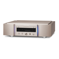
Q102 : XCF01S Q201 : SM5866
1
15
28
14
TSTN
TO
DVDD
SDI
SBCKA
SBCKD
RSTN
IMD1
IMD0
AVSSA
RA
IOUTA
IOUTAN
AVDDA
DI
AVDDB
BCKI
WCKI
DVSS
BCPOL
RB
IOUTB
IOUTBN
AVSSB
DSPOL
CVDD
CVSS
CKI
DSD filter
DSD input interface
BCKI
CVDD
AVSSA
23 level
DEM DAC
23 level
DEM DAC
DVDD
CKI
CVSS
Interpolation
WCKI DI SBCKD SBCKA SDI
Noise shaper
23 level
DEM DAC
23 level
DEM DAC
IOUTB
RB
AVDDB
AVDDA
AVSSB
4568910
3
15
14
16
17
19 20 21 22
26
PCM input interface
DVSS
11
DSPOL
13
12
BCPOL
TO
2
7
RSTN
TSTN
1
IMD1
28
IMD0
27
IOUTBN
18
IOUTA
RA
24 25
IOUTAN
23
Number Name I/O
1
1. Ip = input pin with built-in pull-up resistor
Description
1 TSTN Ip Test mode use only (tie HIGH or leave open for normal operation)
2 TO O Test mode use only (leave open for normal operation)
3 DVDD – Digital supply VDD
4 SDI Ip DSD data input
5 SBCKA Ip DSD bit clock input
6 SBCKD Ip DSD bit clock input (tie LOW for DSD normal input mode)
7 RSTN Ip System reset (active LOW)
8 DI Ip PCM data input
9 BCKI Ip PCM bit clock input
10 WCKI Ip PCM word clock input
11 DVSS – Digital ground VSS
12 BCPOL Ip DSD mode bit clock polarity select
13 DSPOL Ip DSD mode data polarity select
14 CVDD – System clock supply VDD
15 CKI I System clock
16 CVSS – System clock ground VSS
17 AVSSB – B-channel analog ground VSS
18 IOUTBN O B-channel analog output (inverse-phase)
19 IOUTB O B-channel analog output (in-phase)
20 RB I B-channel built-in resistor connection
21 AVDDB – B-channel analog supply VDD
22 AVDDA – A-channel analog supply VDD
23 IOUTAN O A-channel analog output (inverse-phase)
24 IOUTA O A-channel analog output (in-phase)
25 RA I A-channel built-in resistor connection
26 AVSSA – A-channel analog ground VSS
27 IMD0 Ip Input mode select
28 IMD1 Ip Input mode select