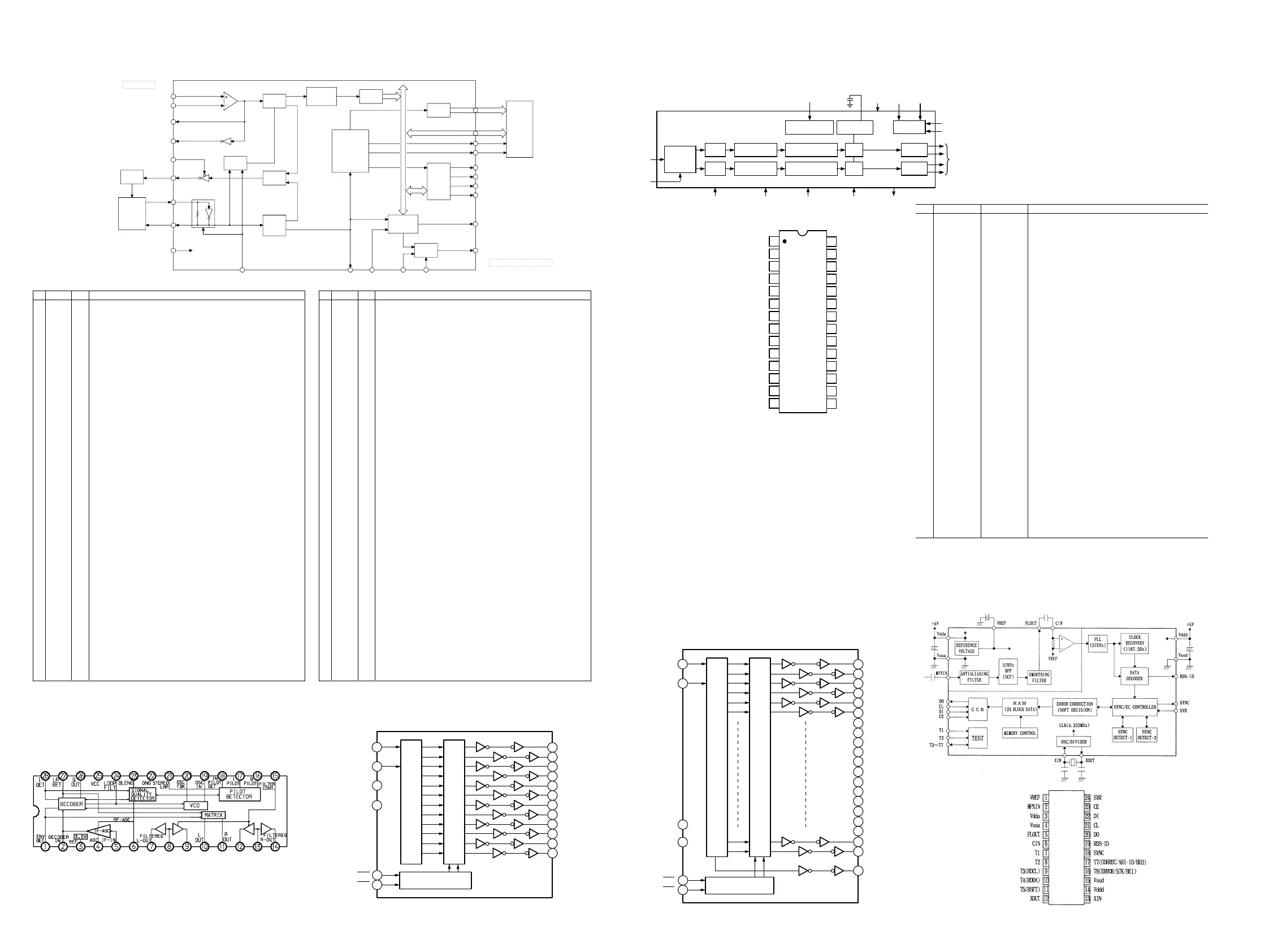
6. IC DATA
Pin Input/Output Pin Name Description
1 I DGND Digital Ground.
2 I MCLK Master Clock Input. Connect to an external clock source at either 256, 384
or 512 F
S
.
3 I CLATCH Latch input for control data. This input is rising-edge sensitive.
4 I CCLK Control clock input for control data. Control input data must be valid on the
rising edge of CCLK. CCLK may be continuous or gated.
5 I CDATA Serial control input, MSB first, containing 16 bits of unsigned data per
channel. Used for specifying channel specific attenuation and mute.
6 I 384/256 Selects the master clock mode as either 384 times the intended sample fre-
quency (HI) or 256 times the intended sample frequency (LO). The state of
this input should be hardwired to logic HI or logic LO, or may be changed
while the AD1855 is in power-down/reset. It must not be changed while the
AD1855 is operational.
7 I X2MCLK Selects internal clock doubler (LO) or internal clock = MCLK (HI).
8 O ZEROR Right Channel Zero Flag Output. This pin goes HI when Right Channel has
no signal input for more than 1024 LR Clock Cycles.
9 I DEEMP De-Emphasis. Digital de-emphasis is enabled when this input signal is HI.
This is used to impose a 50 ms/15 m
s response characteristic on the output
audio spectrum at an assumed 44.1 kHz sample rate.
10 I
96/48
Selects 48 kHz (LO) or 96 kHz Sample Frequency Control.
11, 15 I AGND Analog Ground.
12 O OUTR+ Right Channel Positive line level analog output.
13 O OUTRÐ Right Channel Negative line level analog output.
14 O FILTR Voltage Reference Filter Capacitor Connection. Bypass and decouple the
voltage reference with parallel 10
m F and 0.1 mF capacitors to the AGND.
16 O OUTLÐ Left Channel Negative line level analog output.
17 O OUTL+ Left Channel Positive line level analog output.
18 I AVDD Analog Power Supply. Connect to analog +5 V supply.
19 O FILTB Filter Capacitor connection, connect 10 m
F capacitor to AGND.
20 I IDPM1
Input serial data port mode control one. With IDPM0, defines one of four
serial modes.
21 I IDPM0 Input serial data port mode control zero. With IDPM1, defines one of four
serial modes.
22 O ZEROL Left Channel Zero Flag output. This pin goes HI when Left Channel has no
signal input for more than 1024 LR Clock Cycles.
23 I MUTE Mute. Assert HI to mute both stereo analog outputs. Deassert LO for nor-
mal operation.
24 I PD/RST Power-Down/Reset. The AD1855 is placed in a low power consumption
mode when this pin is held LO. The AD1855 is reset on the rising edge of
this signal. The serial control port registers are reset to the default values.
Connect HI for normal operation.
25 I L/RCLK Left/ Right clock input for input data. Must run continuously.
26 I BCLK Bit clock input for input data. Need not run continuously; may be gated or
used in a burst fashion.
27 I SDATA Serial input, MSB first, containing two channels of 16, 18, 20, and 24 bits of
twos complement data per channel.
28 I DVDD Digital Power Supply Connect to digital +5 V supply.