dsPIC33/PIC24 Family Reference Manual
DS70005340A-page 60 2018 Microchip Technology Inc.
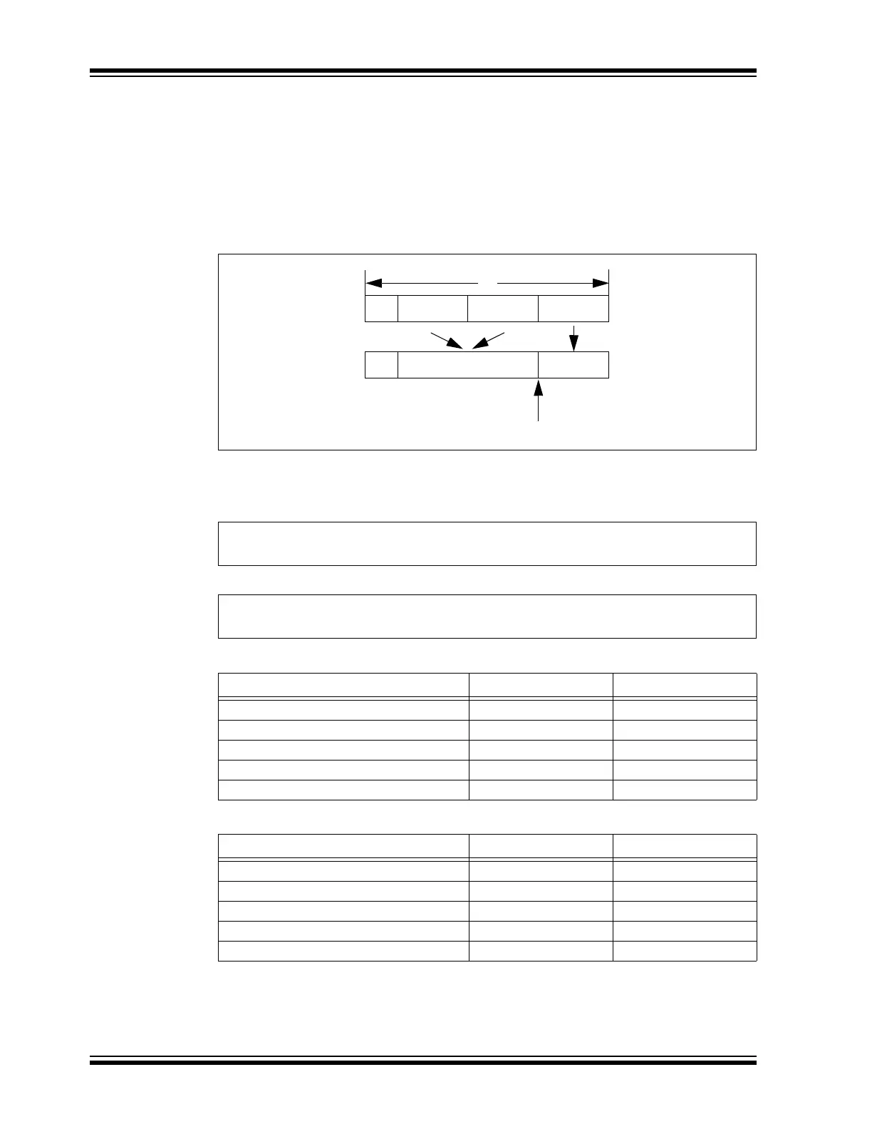
Phase Segment 2 (PHSEG2) – Compensates for errors that may occur due to phase shifts in
the edges. The time segment may be automatically shortened during resynchronization to
compensate for the phase shift.
In the Bit Time registers, PRSEG and PHSEG1 are combined to create TSEG1. PHSEG2 is
called TSEG2. Each segment has multiple Time Quanta (T
Q
). The sample point lies between
TSEG1 and TSEG2.
Table 5-1 and Tabl e 5-2 show the ranges for the bit time configuration parameters.
Figure 5-1: Partition of Bit Time
The total number of T
Q
in a bit time is programmable and can be calculated using Equation 5-5
and Equation 5-6.
Equation 5-5: Number of NTQ in a NBT
Equation 5-6: Number of DTQ in a DBT
Table 5-1: Nominal Bit Rate Configuration Ranges
Table 5-2: Data Bit Rate Configuration Ranges
Segment Min. Max.
NSYNC 1 1
NTSEG1 2 256
NTSEG2 1 128
NSJW 1 128
NTQ per Bit 4 385
Segment Min. Max.
DSYNC 1 1
DTSEG1 1 32
DTSEG2 1 16
DSJW 1 16
DTQ per Bit 3 49
TBIT
SYNC PRSEG PHSEG1 PHSEG2
SYNC TSEG1 TSEG2
Sample Point
NBT
NTQ
------------ NSYNC NTSEG1 NTSEG2++=
DBT
DTQ
------------ D S Y N C D T S E G 1 D T S E G 2++=