91
7521
7521
Plus / N N/B MAINTENANCE
Plus / N N/B MAINTENANCE
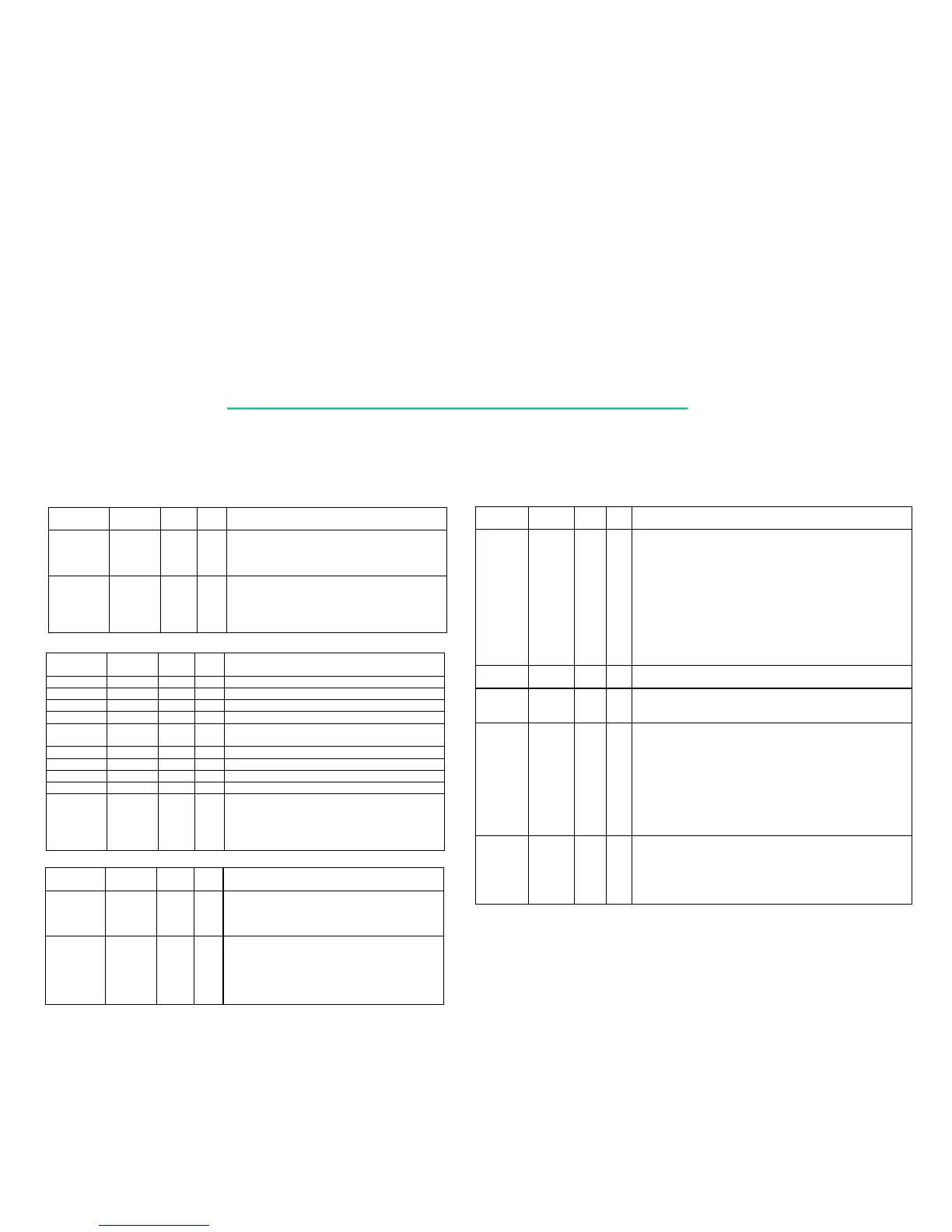
5. Pin Descriptions Of Major Components
5.2 SiS630S Slot 1/Socket 370 2D/3D Ultra-AGP™ Single Chipset
DRAM Controller
Name Tolerance Power
Plane
Type
Attr
Description
SDCLK
3.3V/5V MAIN I SDRAM Clock Input
MD[63:0]
3.3V MAIN I/O System Memory Data Bus
MA[14:0]
3.3V MAIN O System Memory Address Bus
CSA[5:0]#
3.3V MAIN O SDRAM Chip Select
CSB[5:0]#
3.3V MAIN O SDRAM Chip Select Signals
(Duplicated Copy)
DQM[7:0]#
3.3V MAIN O SDRAM Input/Output Data Mask
WE#
3.3V MAIN O SDRAM Write Enable
SRAS#
3.3V MAIN O SDRAM Row Address Strobe
SCAS#
3.3V MAIN O SDRAM Column Address Strobe
CKE
3.3V AUX O SDRAM Clock Enable
During Suspend-to-DRAM mode
(ACPI S2 or S3 state), SDRAM can
be put into self-refresh mode by
asserting CKE.
Host Bus Interface
Name Tolerance Power
Plane
Type
Attr
Description
INIT#
1.5V~5V MAIN OD
Initialization :
INIT is used to re-start the CPU
without flushing its internal caches and registers. In
Pentium II platform it is active high. This signal
requires an external pull-up resistor tied to 3.3V.
A20M#
1.5V~5V MAIN OD
Address 20 Mask :
When A20M# is asserted, the
CPU A20 signal will be forced to "0".
Speed Trap for PII :
This pin will be forced to
voltage level according to the input value of MD42 or
APC0h.5 during system reset period.
Name Tolerance Power
Plane
Ty pe
Attr
Description
AD[31:0]
3.3V/5V MAIN I/O
PCI Address /Data Bus:
In address phase:
1.When the SiS Chip is a PCI bus master, AD[31:0]
are output signals.
2.When the SiS Chip is a PCI target, AD[31:0] are
input signals.
In data phase:
1.
When the SiS Chip is a target of a memory
read/write cycle, AD[31:0] are floating.
2.
When the SiS Chip is a target of a configuration or
an I/O cycle, AD[31:0] are output signals in a
read cycle, and input signals in a write cycle.
PAR
3.3V/5V MAIN I/O
Parity :
SiS630 drives out Even Parity covering AD[31:0] and C/BE[3:0]#. It
does not check the input parity signal.
FRAME#
3.3V/5V MAIN I/O
Frame#:
FRAME# is an output when the SiS Chip is a PCI bus master. The SiS
Chip drives FRAME# to indicate the beginning and duration of an access.
When the SiS Chip is a PCI slave device, FRAME# is an input signal.
IRDY#
3.3V/5V MAIN I/O
Initiator Ready :
IRDY# is an output when the SiS
Chip is a PCI bus master. The assertion of IRDY# indicates the current PCI bus
master's ability to
complete the current data phase of the transaction. For a read cycle, IRDY#
indicates that the PCI bus
master is prepared to accept the read data on the following rising edge of the
PCI clock. For a write
cycle, IRDY# indicates that the bus master has driven valid data on the PCI
bus. When the SiS Chip is a
PCI slave, IRDY# is an input pin.
TRDY#
3.3V/5V MAIN I/O
Target Ready :
TRDY# is an output when the SiS
Chip is a PCI slave. The assertion of TRDY# indicates the target agent's ability
to complete the current data phase of the transaction. For a read cycle, TRDY#
indicates that the target has driven valid data onto the PCI bus. For a write
cycle, TRDY# indicates that the target is prepared to accept data from the PCI
bus. When the SiS Chip is a PCI master, it is an input pin.
PCI Interface
Name Tolerance Power
Plane
Type
Attr
Description
PCICLK
3.3V/5V MAIN I
PCI Clock :
The PCICLK input provides the
fundamental timing and the internal operating
frequency for the SiS Chip. It runs at the same
frequency and skew of the PCI local bus.
C/BE[3:0]#
3.3V/5V MAIN I/O
PCI Bus Command and Byte Enables:
PCI Bus
Command and Byte Enables define the PCI command
during the address phase of a PCI cycle, and the PCI
byte enables during the data phases. C/BE[3:0]#
are outputs when the SiS Chip is a PCI bus master and
inputs when it is a PCI slave.